

Spatially-arranged chemical processing station
a chemical processing station and spatial arrangement technology, applied in the direction of movable spraying apparatus, basic electric elements, coatings, etc., can solve the problems of void formation in metal lines, the size of features must be scaled downward, and the delay of interconnection related time becomes the major limitation, so as to achieve the smallest possible equipment size, the effect of reducing the cost and increasing the system reliability
- Summary
- Abstract
- Description
- Claims
- Application Information
AI Technical Summary
Benefits of technology
Problems solved by technology
Method used
Image

Examples
Embodiment Construction
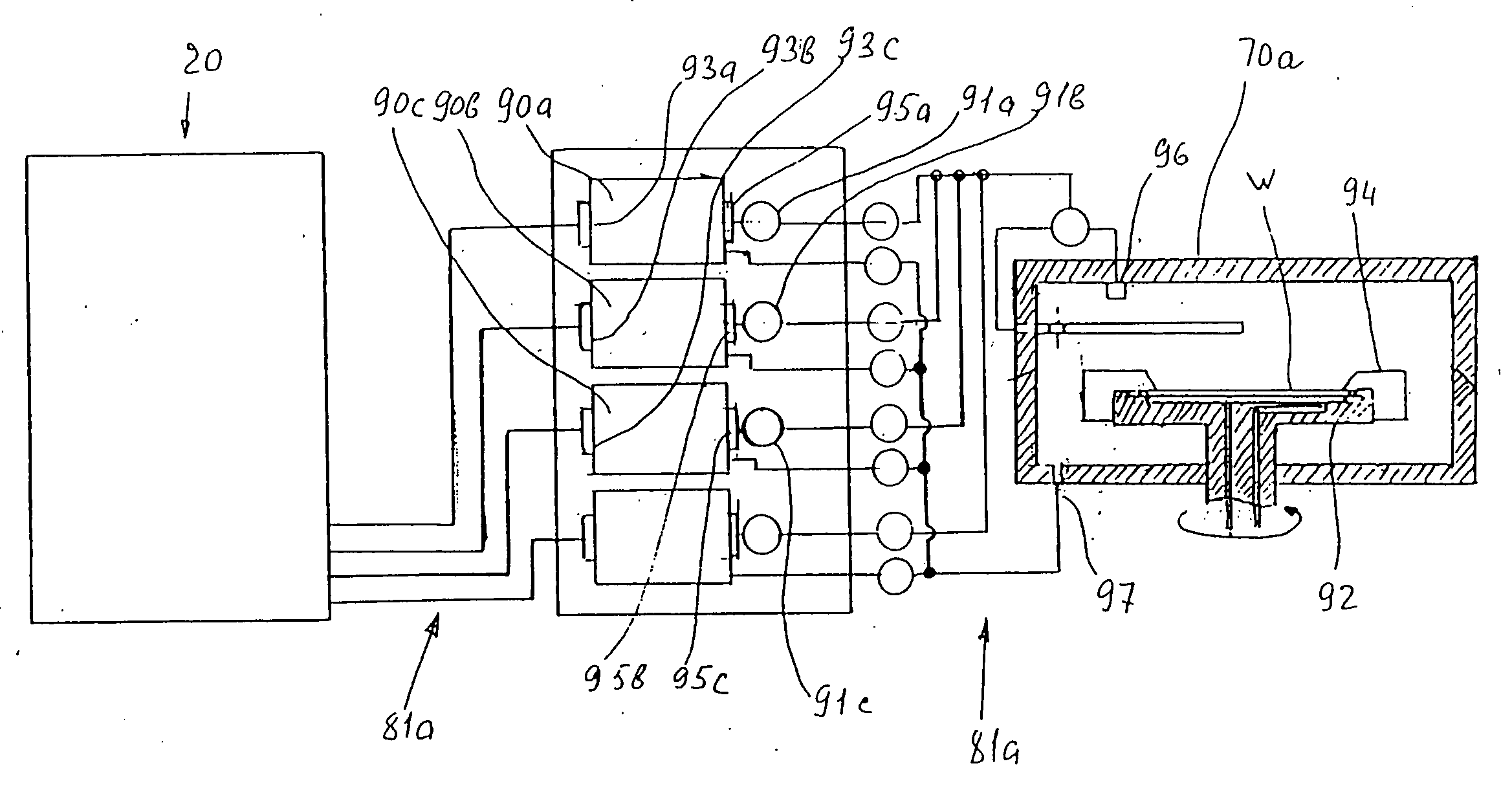
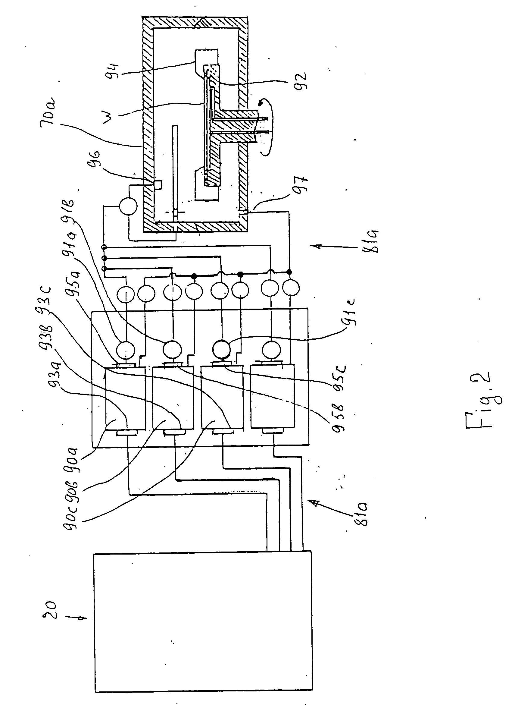
[0030] This invention discloses the equipment configuration which is both novel and flexible, for the electroless deposition of copper, passivation layer, and a barrier layer. The apparatus consists of a number of processing modules and each module in turn a number of process chambers. At least one of the chambers is capable of depositing thin metal films by electroless means. All necessary processing steps for film deposition are performed in a single processing chamber. Thus, the unit provides a way of reducing the number of times the wafer needs to be transferred between wet steps.
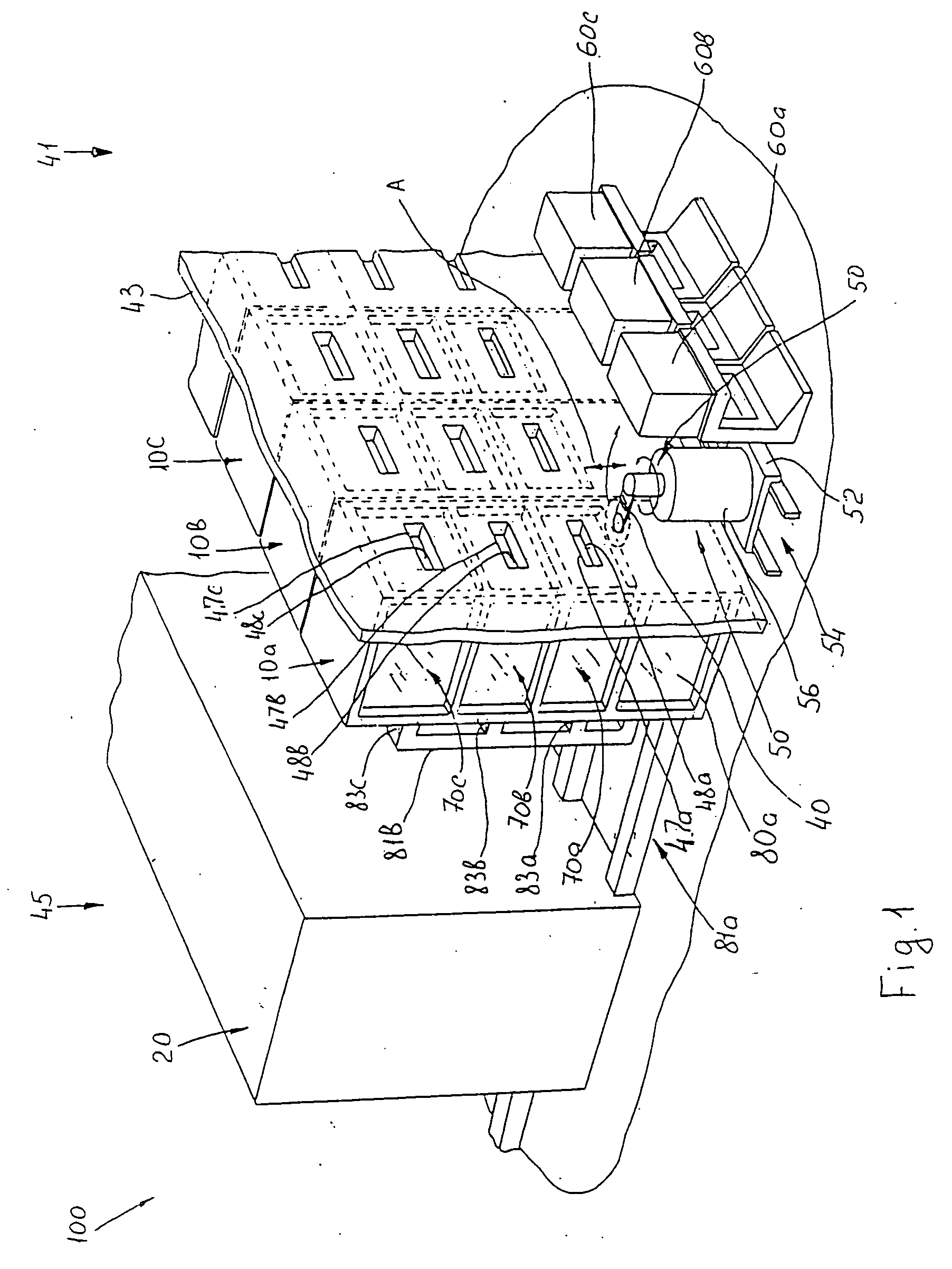
[0031] Reference is made to FIG. 1, which is a three-dimensional general view of a single-wafer electroless deposition station (hereinafter referred to as “system”) of this invention. The system is designated as a whole by the reference numeral 100. The system consists of a multiple number of processing modules 10a, 10b, 10c . . . arranged in a line in a horizontal manner (only three of them are shown)...
PUM
 Abstract
Description
Claims
Application Information