Organic electroluminescence device, conductive laminate and display

a technology of electroluminescent devices and laminates, applied in the direction of organic semiconductor devices, discharge tubes luminescnet screens, conductive layers on insulating supports, etc., can solve the problems of deterioration of el devices or short circuits, work function decreases with time, and inability to secure uniform quality, etc., to achieve large work functions, reduce the drive voltage and increase the lifetime of organic el devices

Inactive Publication Date: 2007-05-10
IDEMITSU KOSAN CO LTD
View PDF5 Cites 17 Cited by
  • Summary
  • Abstract
  • Description
  • Claims
  • Application Information

AI Technical Summary

Benefits of technology

[0013] As described above, JP-A-2001-043980 discloses that a group V or IV metal having a small work function (e.g. Cr, Mo, W, Ta, or Nb) can be used as the anode instead of a metal having a large work function (e.g. Au, Pt, Ni, or Pd). The inventors of the invention found that the work function and the hole injecting efficiency can be increased while utilizing adhesion and microprocessability of the group V or IV metal by adding at least one element selected from lanthanum, cerium, neodymium, samarium, and europium to the group V or IV metal having a small work function (first invention).
[0014] The inventors of the invention also found that a conductive multilayer body having a large work function and exhibiting excellent hole injecting efficiency can be obtained by sputtering using an oxide sintered product containing Ce as a target in a sputtering atmosphere under specific conditions, that is, at a partial pressure of oxygen of 0.1 Pa or less (second invention).
[0015] The inventors of the invention also found that diffusion of metal atoms in the device can be prevented by using two types of metals in combination for the cathode layer, the standard oxidation-reduction potentials of these metals satisfying a specific relationship (third invention).
[0036] According to the invention, since holes are efficiently injected into the emitting layer from the anode, the drive voltage of the organic EL device can be decreased, whereby the lifetime of the organic EL device can be increased.
[0037] Since the conductive multilayer body and the electrode substrate according to the invention have a large work function, a high-luminance organic EL device which shows a small increase in voltage during constant current drive and exhibits a long lifetime can be realized by using the conductive multilayer body or the electrode substrate as an electrode of the organic EL device. According to the method for producing the conductive multilayer body according to the invention, the above-described conductive multilayer body can be efficiently obtained.
[0038] In the organic EL device according to the invention, since metals used for the cathode layer can be prevented from diffusing in the device, deterioration of the device or occurrence of a short circuit due to metal diffusion can be prevented, whereby the lifetime of the EL device can be increased.

Problems solved by technology

However, these methods have a problem in which the work function decreases with time.
Moreover, since it is difficult to uniformly apply oxygen ions over a large area, uniform quality cannot be secured.
However, since Ag diffuses into the emitting layer or the like forming the EL device due to high diffusion (migration) properties, deterioration of the EL device or a short circuit occurs.

Method used


Image

  • Organic electroluminescence device, conductive laminate and display
  • Organic electroluminescence device, conductive laminate and display
  • Organic electroluminescence device, conductive laminate and display

Examples


first embodiment

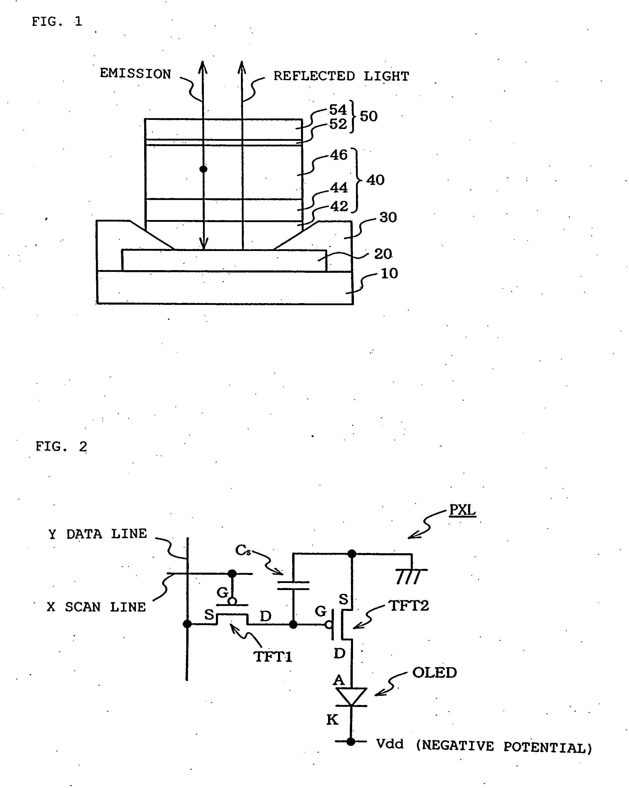
[0050]FIG. 1 is a view showing one embodiment of an organic EL device according to the invention. An anode 20, an insulating layer 30, an emitting layer 40, and a cathode 50 are formed on a substrate 10. The emitting layer 40 includes a hole injecting layer 42, a hole transporting layer 44, and a luminescent medium layer 46. The cathode 20 includes a metal layer 22 and a transparent conductive layer 24. The insulating layer 30 is not indispensable, but is preferably provided in order to prevent a short circuit between the anode 20 and the cathode 50.

[0051] In the luminescent medium layer 46, holes supplied from the anode 20 and electrons supplied from the cathode recombine to emit light. The light is outcoupled upward through the cathode 50.

[0052] According to the first embodiment, at least a part of the anode 40 in contact with the hole injecting layer 42 contains at least one element selected from lanthanum, cerium, neodymium, samarium, and europium, and at least one element sel...

second embodiment

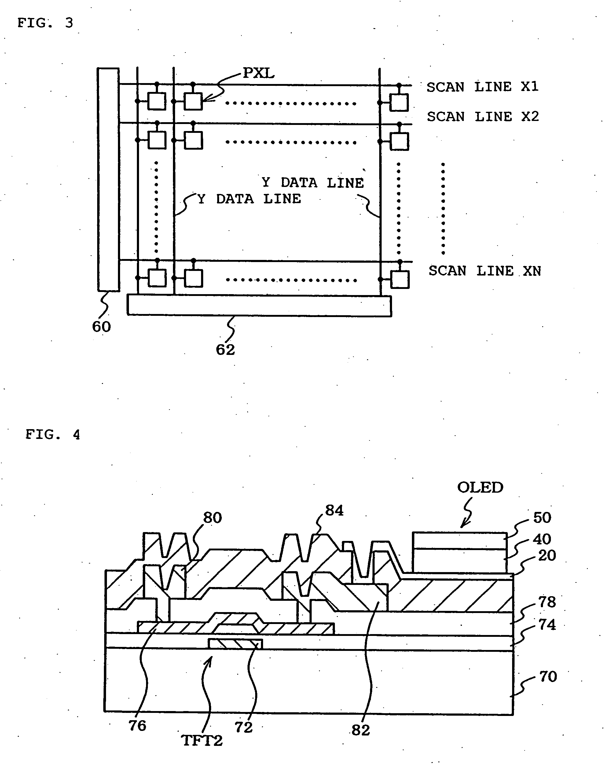
[0057]FIGS. 2, 3, and 4 are views showing one embodiment of a display using the organic EL device according to the invention.

[0058]FIG. 2 is a view showing an equivalent circuit of one pixel of an active matrix type display.

[0059] In the active matrix type display, a number of pixels are arranged in a matrix, and an image is displayed by controlling the light intensity in pixel units corresponding to luminance information provided. In the active matrix type display, current flowing through an organic EL device provided in each pixel is controlled by an active device (generally a thin film transistor (TFT) which is one type of insulated gate type field effect transistor) provided in each pixel.

[0060] A pixel PXL includes an organic EL device OLED, a thin film transistor TFT1 as a first active device, a thin film transistor TFT2 as a second active device, and a storage capacitor Cs. Since the organic EL device generally has rectification properties, it may be called an organic ligh...

third embodiment

[0067]FIG. 5 is a view showing one embodiment of an organic EL device according to the invention.

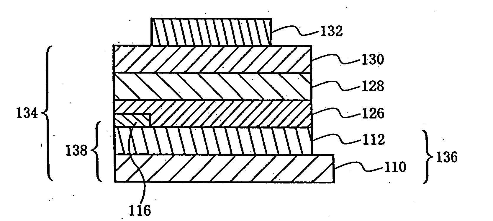
[0068] An organic EL device 134 corresponds to an example of the organic EL device defined in the claims. The organic EL device 134 includes a transparent conductive substrate 138 including a glass substrate 110 and a transparent conductive film 112, a hole transporting layer 126, an organic emitting layer 128, an electron injecting layer 130, and a cathode layer 132.

[0069] A feature of the third embodiment is to produce the transparent conductive substrate 138 including the transparent conductive film 112 having a large work function. Another feature of the third embodiment is to produce the organic EL device 134 which shows a small increase in voltage during constant current drive and exhibits long lifetime and high luminance using the transparent conductive substrate 138 as an electrode.

[0070] Each constituent member and the production method are described below.

A. Conductive Mul...


PUM

PropertyMeasurementUnit
work functionaaaaaaaaaa
binding energyaaaaaaaaaa

Abstract

An organic electroluminescent device including a cathode 50, an anode 20, and an emitting layer interposed between the cathode 50 and the anode 20, at least a part of the anode 20 in contact with the emitting layer 40 containing at least one element selected from lanthanum, cerium, neodymium, samarium, and europium, and at least one element selected from chromium, tungsten, tantalum, niobium, silver, palladium, copper, nickel, cobalt, molybdenum, platinum, and silicon. Since holes are efficiently injected into the emitting layer from the anode, the drive voltage of the organic EL device can be decreased, whereby the lifetime of the organic EL device can be increased.

Description

TECHNICAL FIELD [0001] The invention relates to an organic electroluminescent (EL) device, a conductive multilayer body, a method for producing the conductive multilayer body, an electrode substrate for an organic electroluminescent device, and a display. BACKGROUND ART [0002] An organic EL device includes an anode, a cathode, and an emitting layer placed between the anode and the cathode. The emitting layer includes a luminescent medium layer which emits light upon recombination of holes supplied from the anode and electrons supplied from the cathode. A hole injecting layer and a hole transporting layer are generally provided between the anode and the luminescent medium layer in order to promote injection of holes supplied from the anode. An electron injecting layer and an electron transporting layer are generally provided between the cathode and the luminescent medium layer in order to promote injection of electrons supplied from the cathode. [0003] Since the anode and the cathode...

Claims


Application Information

Patent Timeline
Patent Type & Authority Applications(United States)
IPC IPC(8): H01J63/04H01J1/62B32B7/02B32B9/00H01B5/14H01B13/00H01L51/52H05B33/10H05B33/14H05B33/26H05B33/28
CPCH01L51/5206H01L51/5221H01L2251/5315H05B33/28H05B33/14H05B33/26H01L2251/554H10K50/81H10K50/814H10K50/818H10K50/828H10K2102/3026H10K2101/50H05B33/10
Inventor TOMAI, SHIGEKAZUINOUE, KAZUYOSHISHIBUYA, TADAOSAKAI, TOSHIOMATSUBARA, MASATO
Owner IDEMITSU KOSAN CO LTD
Why Eureka
Try Eureka