

Thin film transistor, manufacturing method for thin film transistor and manufacturing method for display device
a manufacturing method and technology of thin film transistor, applied in the direction of semiconductor devices, basic electric elements, electrical equipment, etc., can solve the problems of not making a contribution to a drastic reduction in the number of steps, inevitably increasing the manufacturing cost, and theoretically difficult to expose a large area substrate having a side of more than 1 meter all at once from a technical standpoint, so as to simplify the manufacturing process and reduce the number of steps of the manufacturing process. , the effect of reducing th
- Summary
- Abstract
- Description
- Claims
- Application Information
AI Technical Summary
Benefits of technology
Problems solved by technology
Method used
Image

Examples
embodiment 1
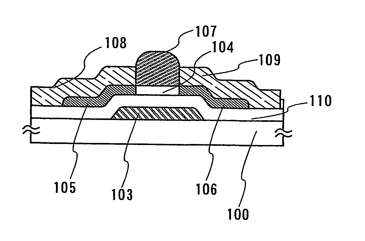
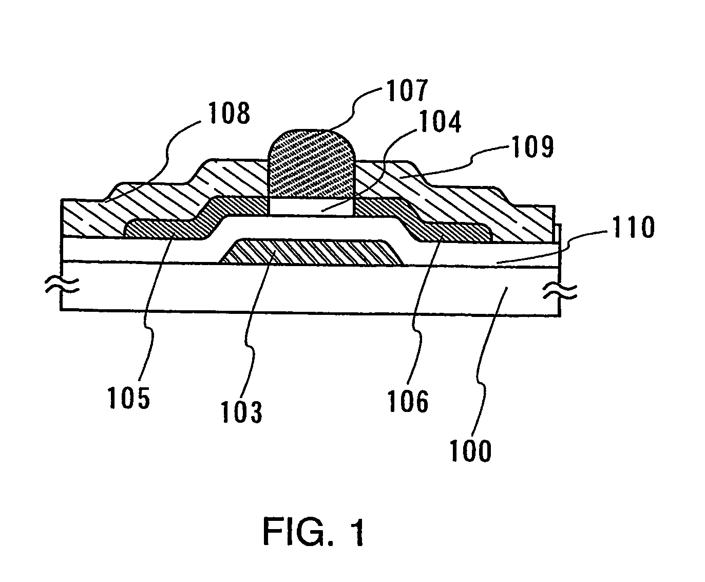
[0044]FIG. 1 is a diagram explaining an embodiment of the present invention and shows a reverse stagger-type (bottom gate-type) TFT. In FIG. 1, 100 denotes a substrate; 103 denotes a gate electrode; 110 denotes a gate insulating film; 104 denotes a channel forming region of a semiconductor layer; 105 denotes a source region; 106 denotes a drain region; 107 denotes a channel protective layer; 108 denotes a source electrode; and 109 denotes a drain electrode.
[0045] Next, a manufacturing process of the reverse stagger-type TFT according to the present invention is explained with reference to FIGS. 3 and 4.
[0046] As for a substrate 300 having an insulating surface, a substrate formed by an insulating substance such as glass, quartz, plastic or alumina, a substrate in which an insulating film of, for example, silicon oxide or silicon nitride is formed on a surface of, for example, a metal such as stainless steel or a semiconductor substrate can be utilized. Further, it is preferable th...
embodiment 2
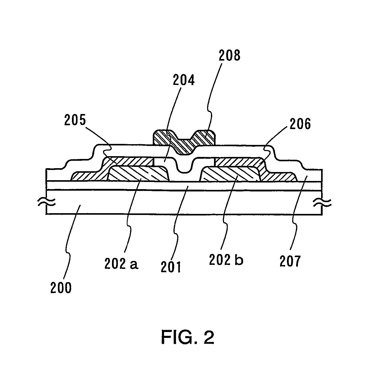
[0064]FIG. 2 is a diagram explaining a positive stagger-type (top gate-type) TFT according to the present invention. In FIG. 2, 200 denotes a substrate; 201 denotes a base film; 202a denotes a source electrode; 202b denotes a drain electrode; 204 denotes a channel forming region of a semiconductor layer; 205 denotes a source region; 206 denotes a drain region; 207 denotes a gate insulating film; and 208 denotes a gate electrode.
[0065] Next, a manufacturing process of the positive stagger-type TFT is explained with reference to FIGS. 5 and 6.
[0066] A base film 501 is formed on a substrate 500 having an insulating surface. As for the substrate 500, a substrate formed by an insulating substance such as glass, quartz or alumina, a substrate in which an insulating film of, for example, silicon oxide or silicon nitride is formed on a surface of, for example, a metal such as stainless steel or a semiconductor substrate can be utilized. Further, a flexible or non-flexible plastic substrat...
example 1
[0082] In the present Example, a manufacturing process of a reverse stagger-type TFT described in Embodiment 1 is explained with reference to FIGS. 3 and 4.
[0083] A W film having a thickness of 100 nm is formed as an electrically conductive film 302 on a substrate 300 by using a sputtering method (see FIG. 3A).
[0084] Next, in order to subjecting the electrically conductive film 302 to patterning, a mask pattern 303 is formed by a droplet discharging method. The mask pattern 303 is formed by selectively discharging a composition comprising polyimide on an electrically conductive film 302 (see FIG. 3B). The composition comprising polyimide discharged on the electrically conductive film 302 is hardened by being baked at 200° C. for 30 minutes. In the present Example, the mask pattern is formed in a film thickness of 600 nm.
[0085] By using the mask pattern 303, the electrically conductive film 302 is subjected to dry etching while using a mixed gas of Cl2, SF6 and O2 as an etching ga...
PUM
 Abstract
Description
Claims
Application Information