Ion implantation device and a method of semiconductor manufacturing by the implantation of boron hydride cluster ions

a cluster ion and ion implantation technology, which is applied in the field of semiconductor manufacturing, can solve the problems of increasing the dispersion of the ion beam, limiting the energy of the conventional ion implantation system at low beam energy, and similar constraints affecting the transport of the low-energy beam, so as to achieve high productivity

Inactive Publication Date: 2007-08-23
SEMEQUIP
View PDF41 Cites 52 Cited by
  • Summary
  • Abstract
  • Description
  • Claims
  • Application Information

AI Technical Summary

Benefits of technology

[0022] An object of this invention is to provide a method of manufacturing a semiconductor device, this method being capable of forming ultra-shallow impurity-doped regions of P-type (i.e., acceptor) conductivity in a semiconductor substrate, and furthermore to do so with high productivity.
[0029] Thus, the implantation of a cluster of n dopant atoms has the potential to provide a dose rate n2 higher than the conventional implant of single atoms. In the case of B18Hx, this maximum dose rate improvement is more than 300. The use of cluster ions for ion implant clearly addresses the transport of low energy (particularly sub-keV) ion beams. It is to be noted that the cluster ion implant process only requires one electrical charge per cluster, rather than having every dopant atom carrying one electrical charge, as in the conventional case. The transport efficiency (beam transmission) is thus improved, since the dispersive Coulomb forces are reduced with a reduction in charge density. Importantly, this feature enables reduced wafer charging, since for a given dose rate, the electrical beam current incident on the wafer is dramatically reduced. Also, since the present invention produces copious amounts of negative ions of boron hydrides, such as B18Hx−, it enables the commercialization of negative ion implantation at high dose rates. Since negative ion implantation produces less wafer charging than positive ion implantation, and since these electrical currents are also much reduced through the use of clusters, yield loss due to wafer charging can be further reduced. Thus, implanting with clusters of n dopant atoms rather than with single atoms ameliorates basic transport problems in low energy ion implantation and enables a dramatically more productive process.

Problems solved by technology

The limitations of conventional ion implantation systems at low beam energy are most evident in the extraction of ions from the ion source, and their subsequent transport through the implanter's beam line.
Similar constraints affect the transport of the low-energy beam after extraction.
In addition, since the electrostatic forces between ions are inversely proportional to the square of the distance between them, electrostatic repulsion is much stronger at low energy, resulting in increased dispersion of the ion beam.
This phenomenon is called “beam blow-up”, and is the principal cause of beam loss in low-energy transport.
In particular, severe extraction and transport difficulties exist for light ions, such as the P-type dopant boron, whose mass is only 11 amu.
In addition, this process also implants fluorine atoms into the semiconductor substrate along with the boron, an undesirable feature of this technique since fluorine has been known to exhibit adverse effects on the semiconductor device.
Process requirements for medium current implants are more complex than those for high current implants.
That is, the transmission efficiency of the ions through the implanter is limited by the emittance of the ion beam.
Presently, the generation of higher current (about 1 mA) ion beams at low (<10 keV) energy is problematic in serial implanters, such that wafer throughput is unacceptably low for certain lower energy implants (for example, in the creation of source and drain structures in leading edge CMOS processes).
Similar transport problems also exist for batch implanters (processing many wafers mounted on a spinning disk) at the low beam energies of <5 keV per ion.
However, prior art ion sources for ion implantation are not effective at producing or preserving ionized clusters of the required N- and P-type dopants.
In general, the wafer throughput of such a system is limited by wafer handling time, which includes evacuating the process chamber and purging and re-introducing the process gas each time a wafer or wafer batch is loader into the process chamber.
Such electron flood systems introduce additional variables into the manufacturing process, and cannot completely eliminate yield losses due to surface charging.
As semiconductor devices become smaller and smaller, transistor operating voltages and gate oxide thicknesses become smaller as well, reducing the damage thresholds in semiconductor device manufacturing, further reducing yield.
Unfortunately, this technology is not yet commercially available, and indeed negative ion implantation has not to the author's knowledge been used to fabricate integrated circuits, even in research and development.

Method used


Image

  • Ion implantation device and a method of semiconductor manufacturing by the implantation of boron hydride cluster ions
  • Ion implantation device and a method of semiconductor manufacturing by the implantation of boron hydride cluster ions
  • Ion implantation device and a method of semiconductor manufacturing by the implantation of boron hydride cluster ions

Examples


Embodiment Construction

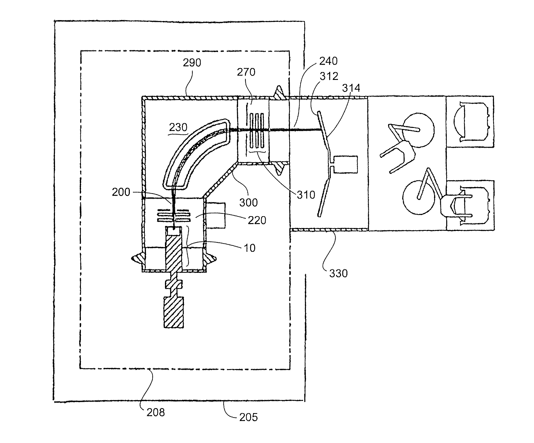
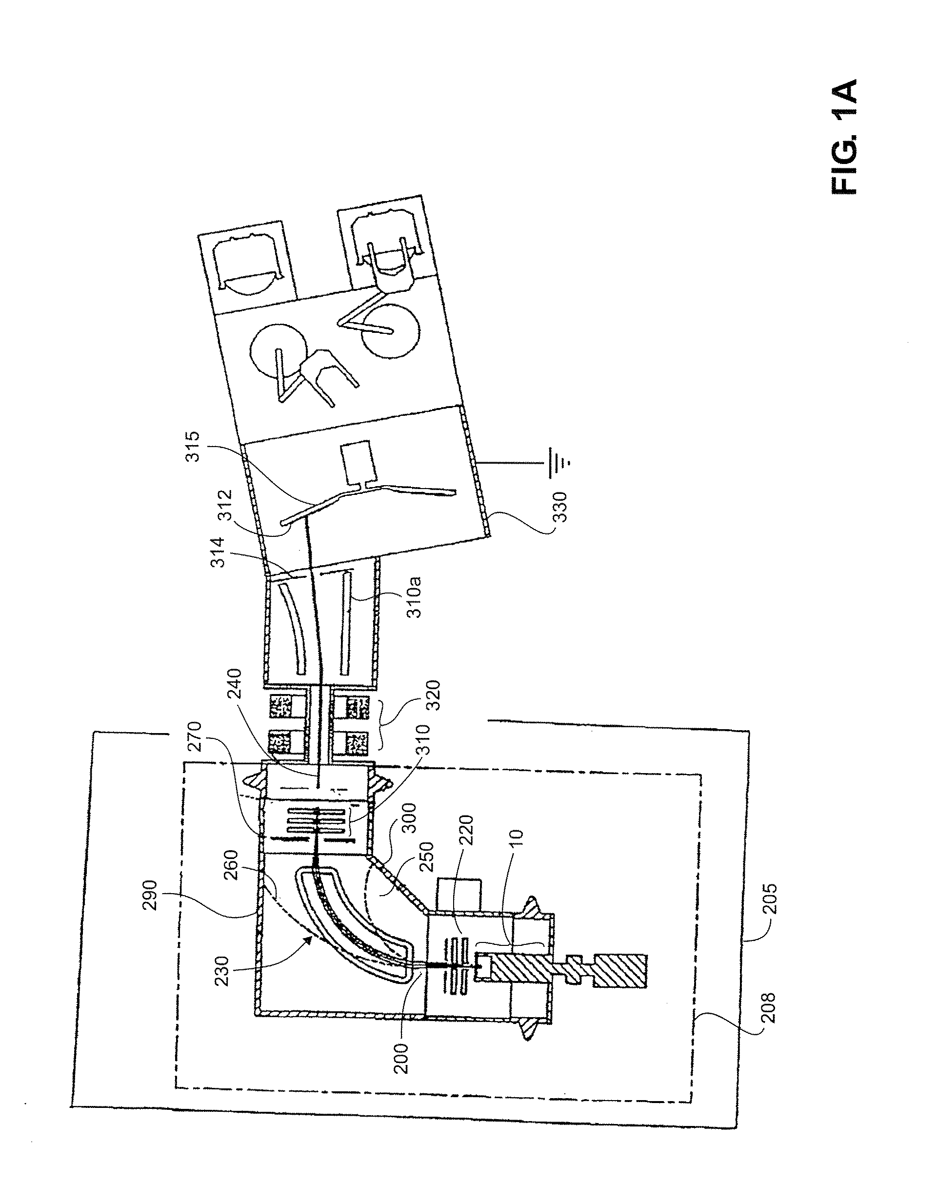
[0069] Cluster Ion Implantation System

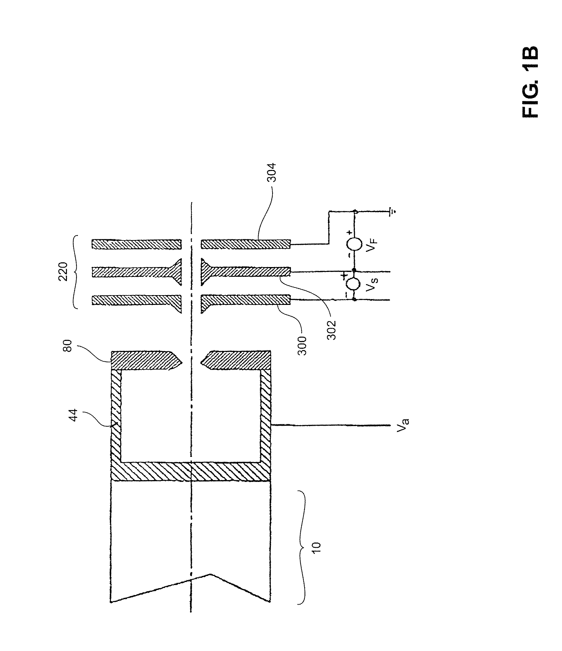
[0070]FIG. 1A is a schematic diagram of a cluster ion implantation system of the high current type in accordance with the present invention. Configurations other than that shown in FIG. 1A are possible. In general, the electrostatic optics of ion implanters employ slots (apertures displaying a large aspect ratio in one dimension) embedded in electrically conductive plates held at different potentials, which tend to produce ribbon beams, i.e., beams which are extended in one dimension. This approach has proven effective in reducing space-charge forces, and simplifies the ion optics by allowing the separation of focusing elements in the dispersive (short axis) and non-dispersive (long axis) directions. The cluster ion source 10 of the present invention is coupled with an extraction electrode 220 to create an ion beam 200 which contains cluster ions, such as B18Hx+ or As4+. The ions are extracted from an elongated slot in ion source 10, called the...


PUM


Abstract

An ion implantation device and a method of manufacturing a semiconductor device is described, wherein ionized boron hydride molecular clusters are implanted to form P-type transistor structures. The molecular cluster ions have the chemical form BnHx+and BnHx−, where 10<n<100 and 0≦x≦n+4. The use of such boron hydride clusters results in a dramatic increase in wafer throughput, as well as improved device yields through the reduction of wafer charging. A method of manufacturing a semiconductor device is further described, comprising the steps of: providing a supply of molecules containing a plurality of dopant atoms into an ionization chamber, ionizing said molecules into dopant cluster ions, extracting and accelerating the dopant cluster ions with an electric field, selecting the desired cluster ions by mass analysis, modifying the final implant energy of the cluster ion through post-analysis ion optics, and implanting the dopant cluster ions into a semiconductor substrate.

Description

CROSS REFERENCE TO RELATED APPLICATIONS [0001] This application is a continuation-in-part of U.S. Provisional Patent Application No. 60 / 463,965, filed on Apr. 18, 2003, entitled “An Ion Implantation Device and a Method of Semiconductor Manufacturing by the Implantation of Boron Hydride Cluster Ions,” and U.S. patent application Ser. No. 10 / 183,768, filed on Jun. 26, 2002, entitled “Electron Impact Ion Source.”BACKGROUND OF THE INVENTION [0002] 1. Field of the Invention [0003] The present invention relates to a method of semiconductor manufacturing in which P-type doping is accomplished by the implantation of ion beams formed from ionized boron hydride molecules, said ions being of the form BnHx+ and BnHx− where 10≦n≦100 and 0≦x≦n+4. [0004] 2. Description of the Prior Art [0005] The Ion Implantation Process [0006] The fabrication of semiconductor devices involves, in part, the introduction of impurities into the semiconductor substrate to form doped regions. The impurity elements are...

Claims


Application Information

Patent Timeline
Patent Type & Authority Applications(United States)
IPC IPC(8): H01J37/08H01J27/20H01J37/317H01L21/00H01L21/265H01L21/336
CPCH01J37/08H01J37/3171H01J37/3172H01L29/6659H01L21/26566H01L21/2658H01L21/26513H01L21/265
Inventor HORSKY, THOMAS N.JACOBSON, DALE C.
Owner SEMEQUIP
Why Eureka
Try Eureka