Isolation structures for integrated circuits and modular methods of forming the same

a technology of integrated circuits and isolation structures, applied in the field of semiconductor chip fabrication, can solve the problems of gate resistance, increased propagation delay, slow switching speed, etc., and achieve the effect of increasing the packing density of semiconductor devices and conserving valuable real esta

Inactive Publication Date: 2007-12-06
ADVANCED ANALOGIC TECHNOLOGIES INCORPORATED +1
View PDF78 Cites 76 Cited by
  • Summary
  • Abstract
  • Description
  • Claims
  • Application Information

AI Technical Summary

Benefits of technology

[0045]The invention also includes implanting a region of the same conductivity type as the substrate between the isolated pockets to help prevent punch-through between adjacent pockets.
[0046]The invention also comprises methods of fabricating the above-referenced isolation structures. The methods are generally modular in the sense that many of the process steps may be performed at different stages of the overall process sequence without significantly affecting the nature of the resulting isolation structure. Moreover, the processes generally do not involve the growth of an epitaxial layer or other processes having significant thermal cycles, which means that the dopant regions remain in an “as implanted” configuration, with minimal lateral and vertical expansion. This permits an increased packing density of the semiconductor devices and conserves valuable real estate on the surface of the semiconductor chip. The methods also include techniques for sharing processing steps in the formation of the various trenches incorporated in the isolation structures, including deep trenches, shallow trenches, dielectric-filled trenches, and trenches filled with conductive material.

Problems solved by technology

While both LOCOS and trench isolation can prevent unwanted surface conduction between devices, they do not facilitate complete electrical isolation.
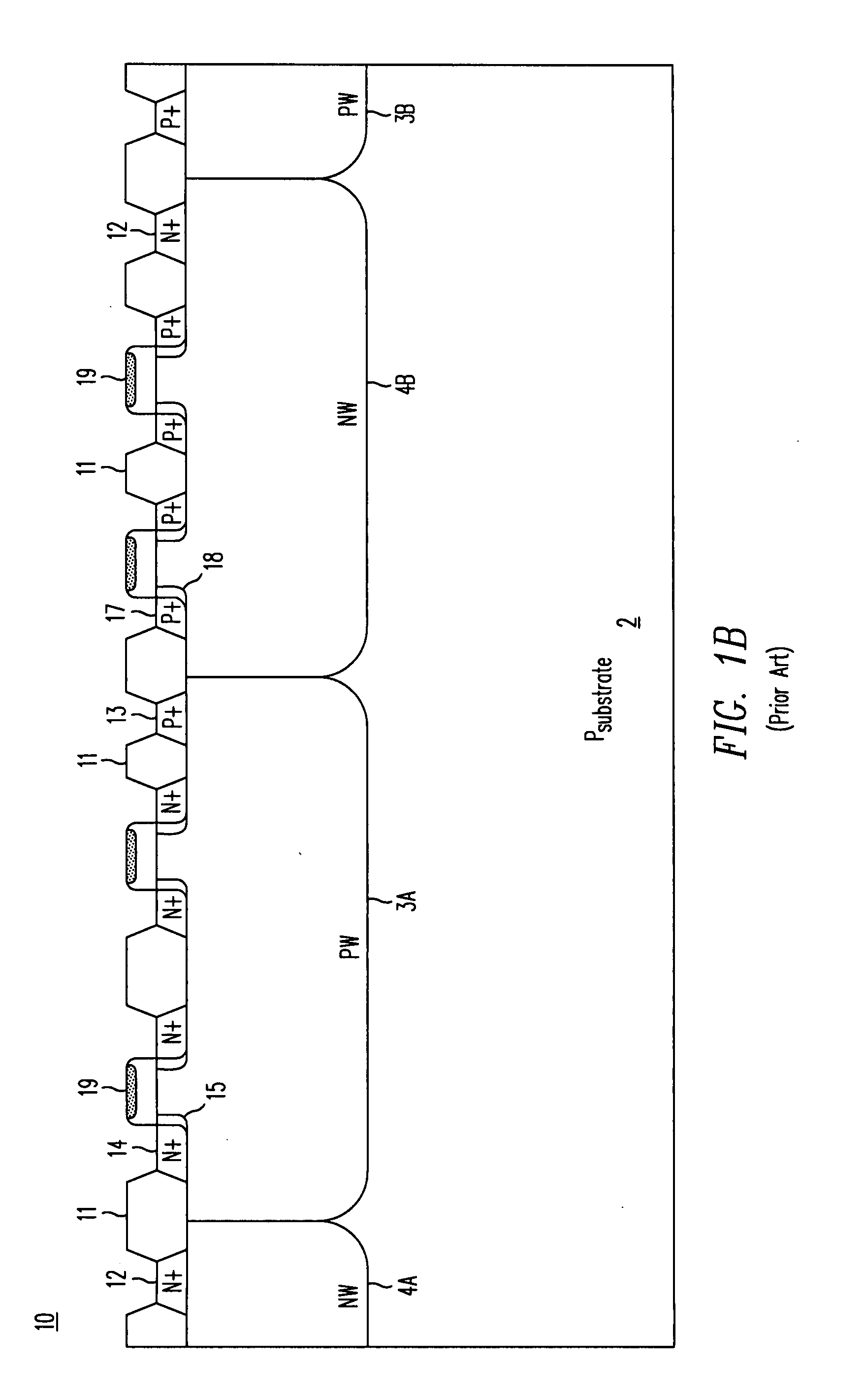
Another limitation of CMOS structure 10 is its gate construction comprising doped polysilicon 19 without any overlying shunting metal.
As transistors are scaled to smaller dimensions, the gate resistance contributes to slower switching speeds and increased propagation delays.
In analog circuitry another major limitation of CMOS 10 is its lack of complete electrical isolation.
Since P-well 3A electrically forms the body (or back gate) of the NMOS transistors, and since P-type substrate 2 is necessarily biased to the most negative on-chip potential (herein referred to as “ground”), then the body connection of every N-channel transistor is biased to ground, limiting their useful operating voltage range and subjecting the N-channel MOSFETs to unwanted substrate noise.
The bird's beak has several unfortunate effects for smaller transistors, affecting the transistor's threshold and gain, and wasting usable real estate.
The problem with both NFD and PFD regions is they diffuse too deep during field oxidation and can adversely impact a transistor's electrical characteristics, especially for deep submicron devices.
The graph shown, however, represents an ideal one-dimensional doping profile and ignores the impact of lateral intrusion under the gate by field dopant or field oxide, both of which alter the two-dimensional and even three-dimensional doping profiles, often in adverse ways.
Scaling the LOCOS to smaller dimensions of thinner final thicknesses is problematic since the shape of the bird's beak becomes sensitive to slight process variations.
One weakness of P-channel 132 is that it inherently includes a substrate-PNP 139, parasitic to the device's construction.
If the gain of the parasitic PNP 139 is too high, especially in the case of lightly-doped shallow N-wells, bipolar snapback breakdown (also known as BVceo or BVcer breakdown) may result and the device may be damaged or destroyed.
Such parasitic ground currents can adversely impact other devices and impair proper circuit operation.
If the same inverter, however, were used to drive an inductor in a Buck switching regulator, diode 153 will become forward-biased whenever P-channel 152 turns off, injecting current into the substrate and potentially causing unwanted phenomena to occur.
A similar problem occurs when using non-isolated CMOS for implementing cascode clamped output driver 160 shown in FIG. 3D.
The problem is that since diode 166 is reverse-biased to a voltage equal to Vout, the threshold of N-channel 162 increases in proportion to the output voltage and thereby limits the circuit's maximum output voltage.
The resulting substrate current can adversely affect efficiency, and cause circuit malfunction.
While not as ideal as dielectric isolation where oxide surrounds each device or circuit, junction isolation has to date offered the best compromise between manufacturing cost and isolation performance.
Growth of epitaxial layer 203 is also slow and time consuming, representing the single most expensive step in semiconductor wafer fabrication.
The isolation diffusion is also expensive, formed using high temperature diffusion for extended durations (up to 18 hours).
Prior to epitaxial growth however, this NBL layer must be diffused sufficiently deep to reduce its surface concentration, or otherwise the concentration control of the epitaxial growth will be adversely impacted.
Because the NBL layer is comprised of a slow diffuser, this pre-epitaxy diffusion process can take more than ten hours.
Since junction isolation fabrication methods rely on high temperature processing to form deep diffused junctions and to grow epitaxial layers, these high temperature processes are expensive and difficult to manufacture, and are incompatible with large diameter wafer manufacturing, exhibiting substantial variation in device electrical performance and preventing high transistor integration densities.
Another disadvantage of junction isolation is the area wasted by the isolation structures and otherwise not available for fabricating active transistors or circuitry.
As a further complication, with junction isolation the design rules (and the wasted area) depend on the maximum voltage of the isolated devices.
In fact unless the PISO opening is sufficient, the isolation may not even reach the substrate.
Obviously, conventional epitaxial junction isolation, despite its electrical benefits, is too area wasteful to remain a viable technology option for mixed signal and power integrated circuits.
While this “epi-less” low thermal budget technique has many advantages over non-isolated and epitaxial junction isolated processes, its reliance on LOCOS imposes certain limitations on its ability to scale to smaller dimensions and higher transistor densities.

Method used


Image

  • Isolation structures for integrated circuits and modular methods of forming the same
  • Isolation structures for integrated circuits and modular methods of forming the same
  • Isolation structures for integrated circuits and modular methods of forming the same

Examples


Embodiment Construction

[0077]The low-temperature isolation process used to fabricate the devices shown in FIG. 6 utilizes high-energy implantation contoured by a LOCOS field oxide layer to achieve the sidewall and floor isolation surrounding each isolated pocket and device. The scaling limitation of such technology and the maximum transistor density, is however, limited by how small a LOCOS field oxide region can be realized. At dimensions much larger than photolithographic limitations, the practical implementation of the LOCOS process becomes manifest. Such adverse effects include distorted field oxide shapes, excessive oxide thinning, high stress, high surface state charge, poor quality gate dielectrics and others. Moreover, as discussed with regard to FIG. 7, small LOCOS dimensions lead to thinning of the implant sidewall isolation regions and a corresponding degradation in the quality of device isolation.

[0078]To eliminate the LOCOS size limitation in scaling ICs, an alternative approach is to utilize...


PUM


Abstract

A variety of isolation structures for semiconductor substrates include a trench formed in the substrate that is filled with a dielectric material or filled with a conductive material and lined with a dielectric layer along the walls of the trench. The trench may be used in combination with doped sidewall isolation regions. Both the trench and the sidewall isolation regions may be annular and enclose an isolated pocket of the substrate. The isolation structures are formed by modular implant and etch processes that do not include significant thermal processing or diffusion of dopants so that the resulting structures are compact and may be tightly packed in the surface of the substrate.

Description

CROSS-REFERENCE TO RELATED APPLICATION[0001]This application is related to application Ser. No. 10 / 262,567, filed Sep. 29, 2002, now U.S. Pat. No. 6,855,985, which is incorporated herein by reference in its entirety.FIELD OF THE INVENTION[0002]This invention relates to semiconductor chip fabrication and in particular to methods of fabricating and electrically isolating bipolar, CMOS and DMOS transistors and passive components in a semiconductor chip monolithically at high densities without the need for epitaxial layers or high temperature fabrication processing steps.BACKGROUND OF THE INVENTION[0003]In the fabrication of semiconductor integrated circuit (IC) chips, it is frequently necessary to electrically isolate devices that are formed on the surface of the chip. There are various ways of doing this. A way is by using the well-known LOCOS (Local Oxidation Of Silicon) process, wherein the surface of the chip is masked with a relatively hard material such as silicon nitride and a t...

Claims


Application Information

Patent Timeline
Patent Type & Authority Applications(United States)
IPC IPC(8): H01L29/00
CPCH01L21/26513H01L29/0649H01L21/76224H01L21/76237H01L21/76243H01L21/76267H01L21/763H01L21/823481H01L21/823878H01L21/823892H01L2924/0002H01L21/761H01L29/0646H01L2924/00H01L21/76
Inventor WILLIAMS, RICHARD K.DISNEY, DONALD RAYCHEN, JUN-WEICHAN, WAI TIENRYU, HYUNGSIK
Owner ADVANCED ANALOGIC TECHNOLOGIES INCORPORATED
Why Eureka
Try Eureka