Gate controlled field emission triode and process for fabricating the same

Inactive Publication Date: 2007-12-13
NATIONAL CHIAO TUNG UNIVERSITY
View PDF2 Cites 26 Cited by
  • Summary
  • Abstract
  • Description
  • Claims
  • Application Information

AI Technical Summary

Benefits of technology

[0005]The object of the present invention is to provide a method for fabricating ZnO nanowires with high aspect ratio as the emitter under low temperature, which could be integrated with the semiconductor process to obtain a gate controlled field emission triode. The method for fabricating ZnO nanowires is the hydrothermal process to be associated with the semiconductor process under the appropriate conditions suitable for nano growth. Thus

Problems solved by technology

However, this method could not fabricate field emission elements with high aspect ratio, and thus could not provide high field enhancement factor for the field emission emitter implemented in optoelectronic device accordingly.
), so they are not easily integrated into the semiconductor process.
Simultaneously, they lack of sufficient uniformity reaction for large area production, and are not suitable for the fabrication of large-scale device.
The problems of prior art at least include: employing high pollution metals, such as Fe, Co, Ni, in the semiconductor process, wherein these metals are easy to make the

Method used


Image

  • Gate controlled field emission triode and process for fabricating the same
  • Gate controlled field emission triode and process for fabricating the same
  • Gate controlled field emission triode and process for fabricating the same

Examples


Embodiment Construction

[0022]In the text which follows, the invention is described by way of example on the basis of the following exemplary embodiments:

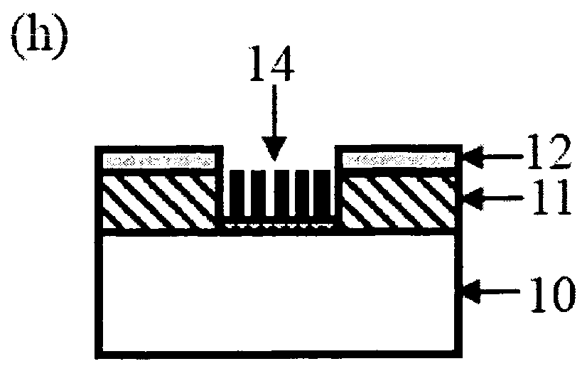
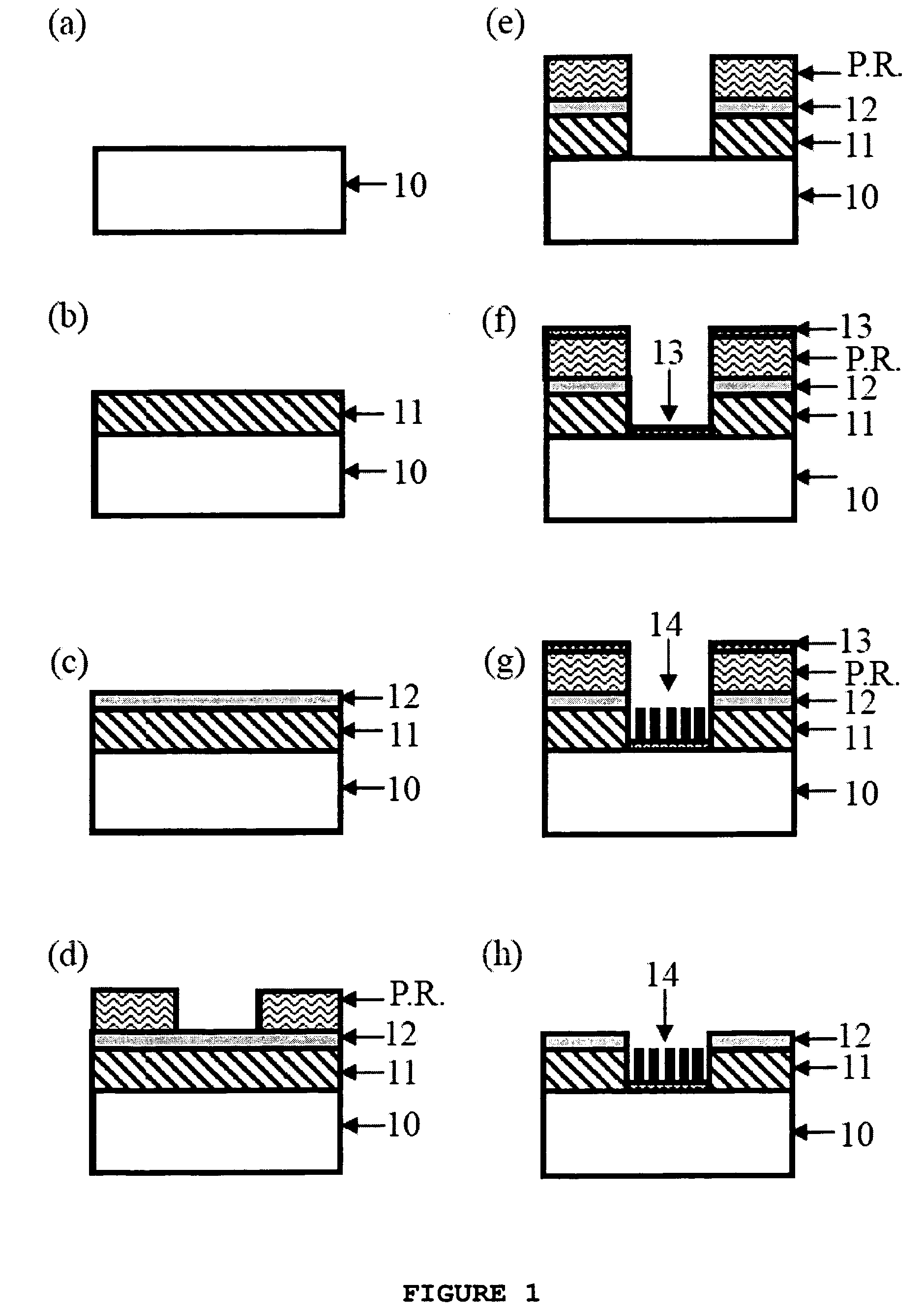
[0023]As shown in FIG. 1, (a) using a silicon substrate 10 as the support base of devices, and in order to enhance the adhesion between the substrate and the device film, conducting normal semiconductor R.C.A cleaning on the silicon substrate; (b) placing the substrate in the chamber for employing the Plasma Enhanced Chemical Vapor Deposition (PECVD) to fabricate the dielectric layer of SiO2 11 film; (c) conducting the evaporation deposition of aluminum film 12 for the gate electrode; (d) coating the photoresist on the film surface; (e) employing exposure and etching to sequentially etch the gate electrode layer and the dielectric layer to form a cavity; (f) employing the photoresist as a mask on the surface and using the sputtering method to deposit ZnO seeding layer 13 on the substrate surface and then removing the photoresistance layer, in which the un...


PUM


Abstract

This invention relates to a process for fabricating ZnO nanowires with high aspect ratio at low temperature, which is associated with semiconductor manufacturing process and a gate controlled field emission triode is obtained. The process comprises providing a semiconductor substrate, depositing a dielectric layer and a conducting layer, respectively, on the semiconductor substrate, defining the positions of emitter arrays on the dielectric layer and conducting layer, depositing an ultra thin ZnO film as a seeding layer on the substrate, growing the ZnO nanowires as the emitter arrays by using hydrothermal process, and etching the areas excluding the emitter arrays, then obtaining the gate controlled field emission triode.

Description

FIELD OF THE INVENTION[0001]The present invention relates to a method for fabricating field emission elements with high aspect ratio ZnO synthesized by low temperature processing technique, and particularly to a method for significantly improving the field emission ability of field emission triode.BACKGROUND OF THE INVENTION[0002]Currently, the fabrication of field emission emitter of optoelectronic device mainly employs the association of lithography and etching process of the typical semiconductor manufacturing for making the pyramidal emitter. However, this method could not fabricate field emission elements with high aspect ratio, and thus could not provide high field enhancement factor for the field emission emitter implemented in optoelectronic device accordingly. Therefore, it would normally require higher driving voltage for the emitter to trigger the electrons. Some relevant researches employed the high aspect ratio nano-structure as the field emitter, such as carbon nanotub...

Claims


Application Information

Patent Timeline
IPC IPC(8): H01L29/12H01L21/00
CPCH01J1/304H01J2201/30446H01J9/025
Inventor TSENG, TSEUNG-YUENLEE, CHIA-YINGLI, SEU-YILIN, PANG
Owner NATIONAL CHIAO TUNG UNIVERSITY
Why Eureka
Try Eureka