Transparent conducting oxide thin films and related devices

a technology of conducting oxide and conducting oxide, applied in the direction of discharge tube/lamp details, natural mineral layered products, synthetic resin layered products, etc., can solve the problems of increasing the price of indium, the generation of flat panel display and photovoltaic technologies, and the supply deficit of indium, so as to achieve enhanced chemical vapor deposition, simple procedures, and satisfactory surface smoothness

Active Publication Date: 2008-01-31
NORTHWESTERN UNIV
View PDF1 Cites 17 Cited by
  • Summary
  • Abstract
  • Description
  • Claims
  • Application Information

AI Technical Summary

Benefits of technology

[0070] In certain embodiments, the ZITO thin films are solid solutions of In2O3, SnO2 and ZnO. As mentioned above, it was found that a phase-pure bixbyite structure can be retained in ZITO thin films with an indium content as low as about 40 cation %. It was found that Zn and Sn reach their solubility limit at about x=about 1.8 and y=about 1.7, and a second ZnO phase was detected in some embodiments.
[0071] Atomic force microscopy shows that the ZITO thin films can have satisfactory surface smoothness, with room-mean-square (RMS) roughness less than or equal to 2% of the film thickness. In certain embodiments, the RMS is less than or equal to 5 nm.
[0072] In addition to the desirable properties described above, ZITO thin films can also exhibit appreciable chemical inertness. It typically requires more than 1 hour to dissolve a 200 nm thick ZITO film in concentrated hydrochloric acid, while less than 15 minutes are required for a commercial 130 nm thick ITO film. Accordingly, ZITO thin films of the invention can offer multiple desirable properties compared to previous ITO and ZITO materials.
[0073] 2. Processes for Producing Transparent Conducting Oxide Thin Films
[0074] Various deposition processes have been used to produce TCO thin films. They include various physical and chemical deposition techniques. Non-limiting examples of physical deposition techniques include sputtering, pulsed laser deposition and vacuum evaporation. Examples of chemical deposition techniques include, but are not limited to, ion plating and chemical vapor deposition such as metal-organic chemical vapor deposition (MOCVD) and plasma enhanced chemical vapor deposition (PECVD). Non- limiting examples of deposition processes that involve a mixture of chemical and physical means include reactive sputtering and molecular beam epitaxy (MBE).
[0075] Sputtering is an effective process for forming a film of a compound of low vapor pressure on a substrate, or forming a film whose thickness needs to be precisely controlled. It has been widely used because of its relatively simple procedures. Typically, a gaseous plasma is generated in a vacuum chamber to provide energetic ions. These ions bombard against the surface of a solid target and eject its atoms into the gas phase. Film growth is achieved by deposition of the sputtered atoms on the substrate.

Problems solved by technology

Furthermore, due to recent high demands for flat panel displays, there has been a growing supply deficit for indium.
As a result, the price of indium has increased drastically.
This presents significant challenges to large-scale introduction of next- generation flat panel display and photovoltaic technologies, as commercial ITO thin films often have indium content near 90 cation %.
However, the chemical and electronic properties of ITO are far from optimum for current and future generation OLEDs.
However, all such materials suffer from some combination of poor optical transparency and / or significantly lower work functions than ITO, resulting in poor Fermi level energetic alignment with HTL HOMOs.
For example, while zinc is an important component in many new TCO materials, current zinc precursors for MOCVD processes suffer from either poor reproducibility in growth processes or chemical instability.
However, diethyl zinc and dimethyl zinc are volatile, pyrophoric liquids which must be handled in an inert atmosphere.
They are highly reactive materials and difficult to control in the deposition of multi-component films.
However, it is a solid over a broad temperature range and suffers from sintering at elevated temperatures and during film growth runs.
Sintering decreases the surface area of the solid precursor and thereby causes the flux of gaseous zinc species being transported to vary during the film growth process, seriously compromising film compositional control.

Method used


Image

  • Transparent conducting oxide thin films and related devices
  • Transparent conducting oxide thin films and related devices
  • Transparent conducting oxide thin films and related devices

Examples


example 1

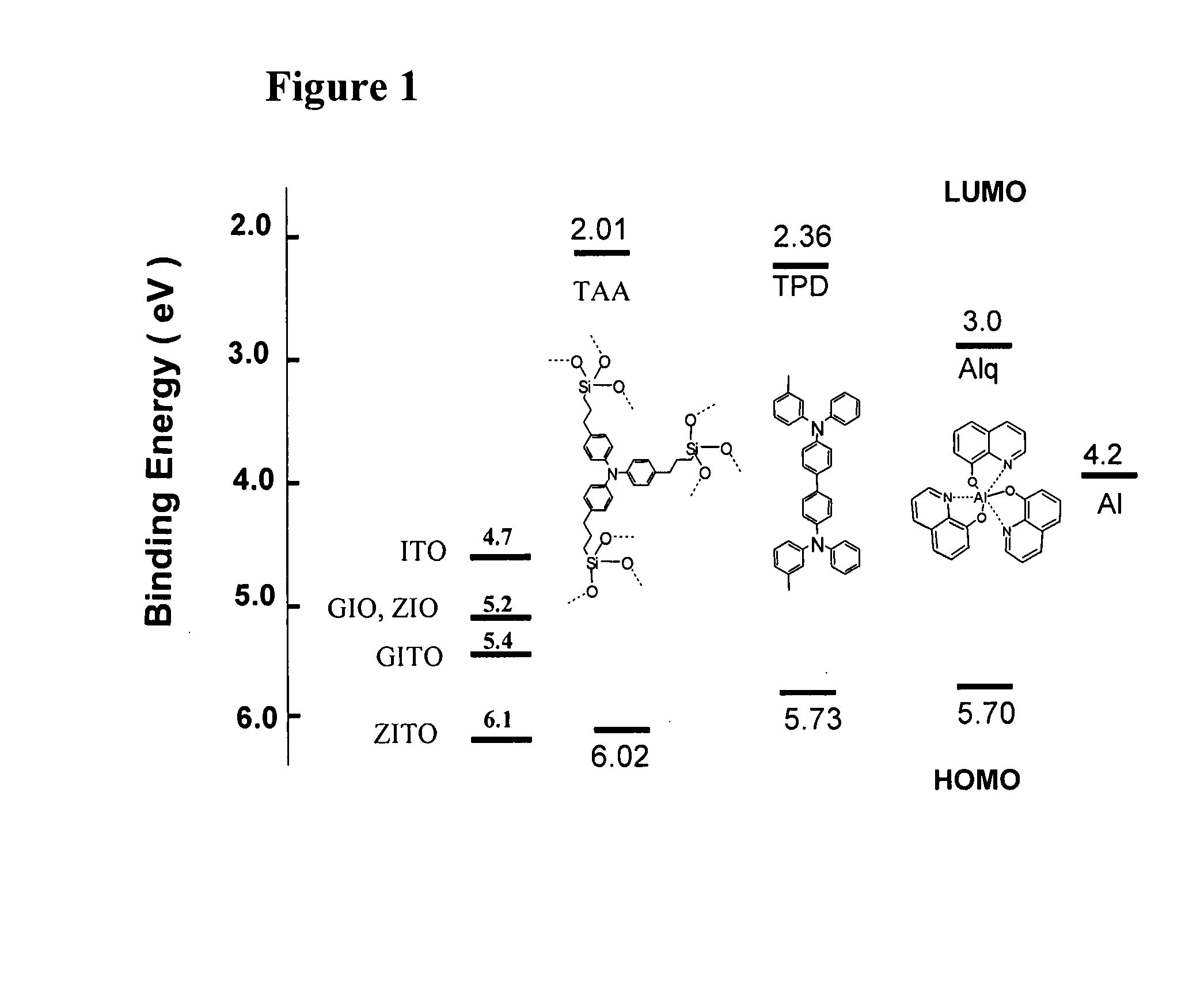
[0106] Growth conditions (MOCVD) on float glass substrates and characterization of ZITO, ZIO, GITO, and GIO thin films by X-ray diffraction, SEM, TEM, and AFM, as well as by other compositional, electrical, and microstructural techniques have been described previously. Microstructurally, all have homogeneously doped cubic In2O3 bixbyite crystal structures, and surface rms roughnesses comparable to commercial ITO. Effective work functions were determined by UV spectroscopy using the 21.8 eV He (I) source (Omicron H1513) of a Kratos Axis-Ultra 165 photoelectron spectrometer. (R. Schlaf, B. A. Parkinson, P. A. Lee, K. W. Nebesny, N. R. Armstrong, Appl. Phys. Lett. 1998, 73, 1026.) Work functions were obtained by lightly sputtering the TCO surface with an Ar+ beam (1 keV), to remove adventitious impurities (as revealed by XPS) and then recording the difference in energy between the high kinetic energy onset and the low kinetic energy cutoff for photoionization. Samples were biased at −5...

example 2

[0107] Relevant properties of several TCO anodes of this invention are summarized in Table 1, below. Note that all have lower optical absorption coefficients than commercial ITO (Donelley Corp., 20 Ω / □). The visible transparency windows of these films are also significantly broader than that of ITO. (A. Wang, N. L. Edleman, J. R. Babcock, T. J. Marks, M. A. Lane, P. W. Brazis, C. R. Kannewurf, i Mater. Res. Soc. Symp. Proc. 2000, 607, 345.) Although ZIO and GIO have somewhat lower n-type conductivities (700-1000 S / cm) than commercial ITO (˜3000 S / cm), the Sn-doped versions (GITO, ZITO) exhibit comparable values (2000-3300 S / cm). As currently understood, GITO and ZITO are the most transparent and among the most conductive TCO materials available for OLED fabrication. In terms of robustness, all of the present films are more chemically, inert than commercial ITO; e.g., to remove a 120 nm thick ITO film using 20% aqueous HCl at 25° C. requires ˜5 min, while comparable degradation of GI...

example 3

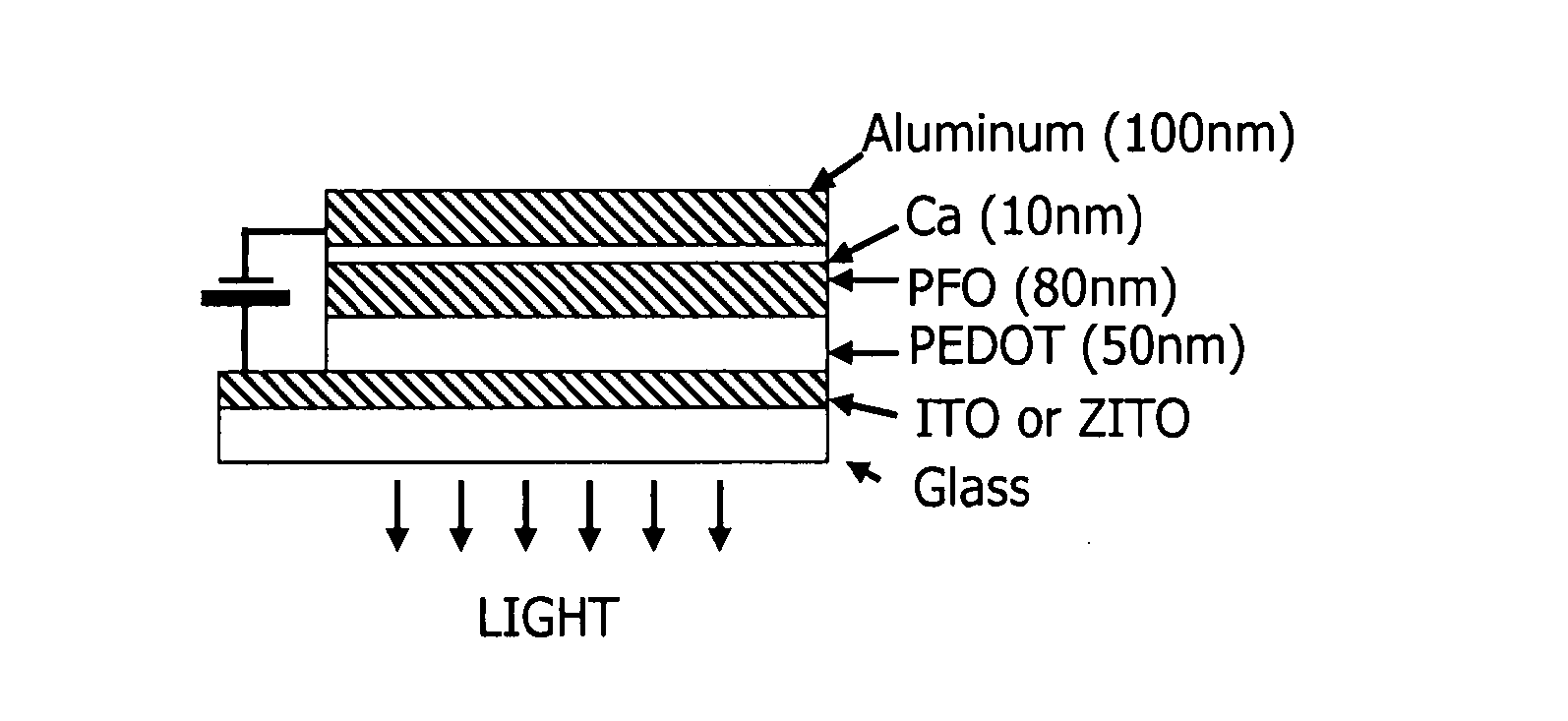
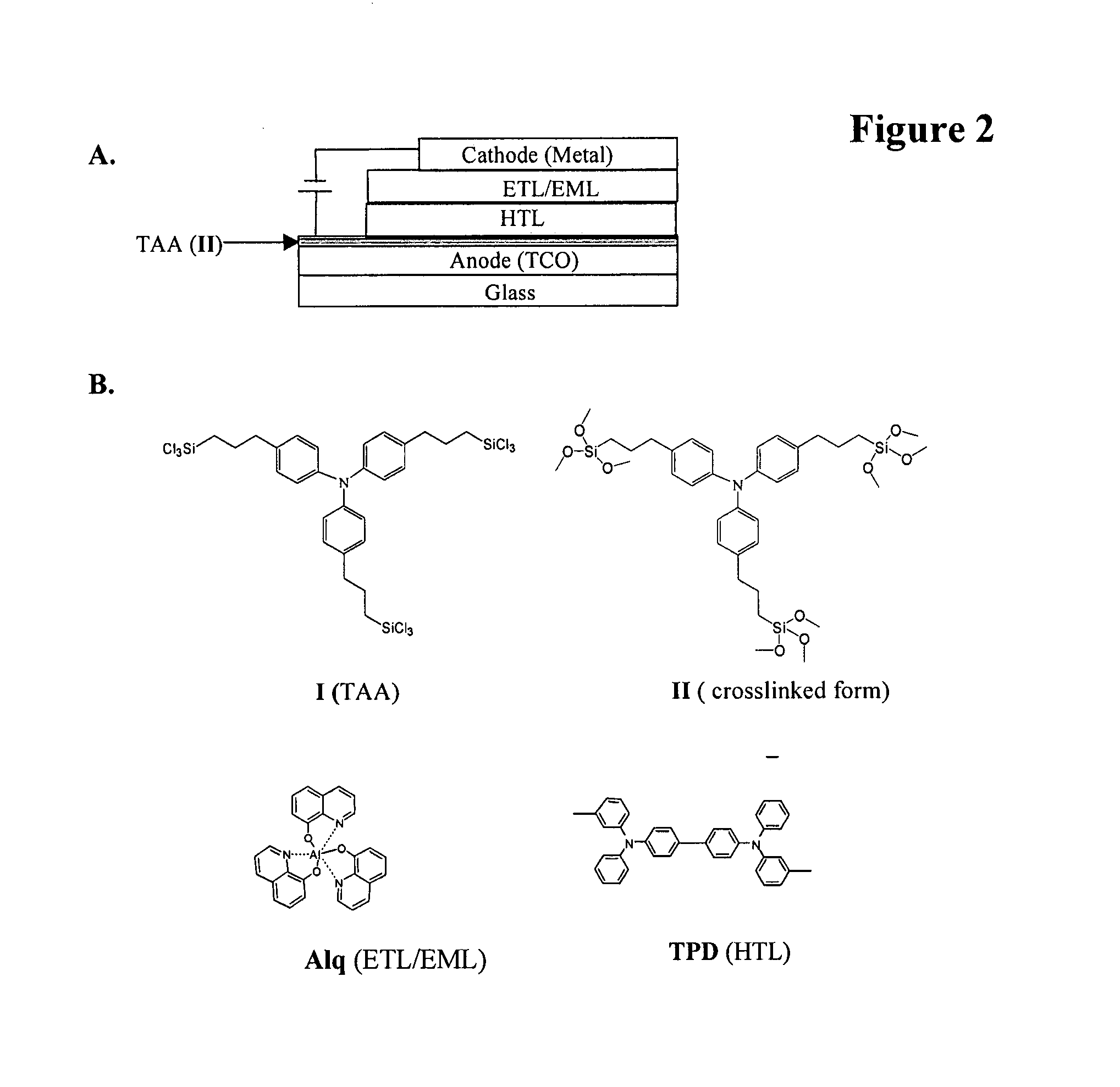
[0108] For OLED fabrication, the as-grown TCO and commercial ITO films were subjected to identical sequential cleaning with HPLC grade acetone, isopropanol, and methanol, then with an oxygen plasma to eliminate organic residues. All of the freshly cleaned metal oxide surfaces are highly hydrophilic as evidenced by advancing aqueous contact angles of 0°. A thin, crosslinked TAA layer derived from N(4-C6H4CH2CH2CH2SiCl3)3 (I, FIG. 2) was then spin-coated onto each of the anode surfaces from a 1 mM toluene solution and cured at 120° C. for 1.0 hour. This layer has been shown in previous work to enhance TCO / HTL interfacial cohesion and charge injection efficiency. The TAA films are robust, adherent, contiguous, and electroactive, with ˜1.5 nm RMS roughness on all TCO substrates, and having a thickness of ˜15 nm (by X-ray reflectivity.) (W. Li, J. E. Malinsky, H. Chou, W. Ma, L. Geng, T. J. Marks, G. E. Jabbour, S. E. Shaheen, B. Kippelen, N. Pegyhambarian, A. J. R. P. Dutta, J. Anderson...


PUM

PropertyMeasurementUnit
conductivityaaaaaaaaaa
thicknessaaaaaaaaaa
thicknessaaaaaaaaaa

Abstract

Transparent conducting oxide thin films having a reduced indium content and/or an increased tin content are provided. In addition, processes for producing the same, precursors for producing the same, and transparent electroconductive substrate for display panels and organic electroluminescence devices, both including the transparent conducting oxide thin films, are provided.

Description

[0001] This application claims priority benefit of provisional application Ser. No. 60 / 784,658, filed on Mar. 22, 2006, the entirety of which is incorporated herein by reference, and claims priority from and is a continuation in part of application serial no. 10 / 228,521, filed on Aug. 27, 2002, which claims priority benefit of provisional application Ser. No. 60 / 315,159, filed Aug. 27, 2001, each of which is incorporated herein by reference in its entirety[0002] The United States government has certain rights to this invention pursuant to Grant Nos. CHE-0201767 and DMR-0076097 from the United States National Science Foundation and Grant No. N00014-95-1-1-1319 from the Office of Naval Research, all to Northwestern University.BACKGROUND [0003] Transparent conducting oxide (TCO) thin films have wide applications in optoelectronics. For example, they have been widely used as transparent electrodes in various devices including flat panel displays such as liquid crystal displays (LCDs) an...

Claims


Application Information

Patent Timeline
Patent Type & Authority Applications(United States)
IPC IPC(8): H01L51/54B29C71/02B32B17/06B32B9/04C07F3/06C23C16/40H01B1/08
CPCC03C17/36C03C2217/948C07F3/003Y10T428/10C23C16/56H01B1/08H01L51/5206C23C16/407C09K2323/00H10K50/81H10K2101/00
Inventor MARKS, TOBIN J.NI, JUNWANG, ANCHUANYANG, YUMETZ, ANDREWJIN, SHUWANG, LIAN
Owner NORTHWESTERN UNIV
Why Eureka
Try Eureka