

Formulations for cleaning memory device structures
a memory device and structure technology, applied in the preparation of detergent mixture compositions, inorganic non-surface active detergent compositions, detergent compounding agents, etc., can solve the problems of increasing the difficulty of fabricating stacked or trench storage capacitors with sufficient capacitance, increasing parasitic capacitance, and reducing the performance (speed) of dram circuits
Inactive Publication Date: 2008-05-29
ADVANCED TECH MATERIALS INC
View PDF29 Cites 77 Cited by
- Summary
- Abstract
- Description
- Claims
- Application Information
AI Technical Summary
Problems solved by technology
Unfortunately, as the cell size decreases, it becomes increasingly more difficult to fabricate stacked or trench storage capacitors with sufficient capacitance to store the necessary charge to provide an acceptable signal-to-noise level for the read circuits (sense amplifiers) to detect.
This increase in refresh cycles further reduces the performance (speed) of the DRAM circuit.
This results in increased parasitic capacitance between adjacent capacitors and can disturb the data retention (charge) on the capacitor.
Removing the capping and the insulating layers using a wet clean has been challenging because the aspect ratio of the cylindrical features (i.e., the ratio between the height of the cylinder and the width of the cylinder) is very high, typically greater than 5:1.
There are several technological disadvantages to using aqueous-based wet cleaning solutions.
Water has a high surface tension which limits or prevents access to the smaller image nodes with high aspect ratios, and therefore, removing the residues from the crevices or grooves becomes very difficult.
In addition, aqueous-based etchant formulations often leave once dissolved solutes behind in the trenches and / or vias upon evaporative drying, which inhibit conduction and reduce device yield.
Furthermore, porous low-k dielectric materials do not have sufficient mechanical strength to withstand the destructive forces (capillary stress) of high surface tension liquids, resulting in pattern collapse of the structures.
SCFs are highly non-polar and as such, many species, including polar and non-polar species, are not adequately solubilized therein.
Method used
View moreImage
Smart ImageViewing Examples

Examples
example a
[0075]Pyridine:HF (30%:70%): 7.5 wt %; Sulfolane: 10.3 wt %; Butyl carbitol: 82.2 wt %
example b
[0076]Pyridine:HF (30%:70%): 7.5 wt %; Sulfolane: 10.3 wt %; Butyl carbitol: 57.2 wt %; Propylene carbonate: 25.0 wt %
example c
[0077]Pyridine:HF (30%:70%): 7.5 wt %; Sulfolane: 10.3 wt %; Propylene carbonate: 82.2 wt %
Login to View More PUM
| Property | Measurement | Unit |
|---|---|---|
| surface tension | aaaaa | aaaaa |
| surface tension | aaaaa | aaaaa |
| wt % | aaaaa | aaaaa |
Abstract
A removal composition and process for removing silicon-containing layers from a microelectronic device having said layers thereon. The removal composition selectively removes layers including, but not limited to, silicon oxide, plasma enhanced tetraethyl orthosilicate (P-TEOS), borophosphosilicate glass (BPSG), plasma enhanced oxide (PEOX), high density plasma oxide (HDP), phosphosilicate glass (PSG), spin-on-dielectrics (SOD), thermal oxide, updoped silicate glass, sacrificial oxides, silicon-containing organic polymers, silicon-containing hybrid organic / inorganic materials, organosilicate glass (OSG), TEOS, fluorinated silicate glass (FSG), hemispherical grain (HSQ), carbon-doped oxide (CDO) glass, and combinations thereof, relative to lower electrode, device substrate, and / or etch stop layer materials.
Description
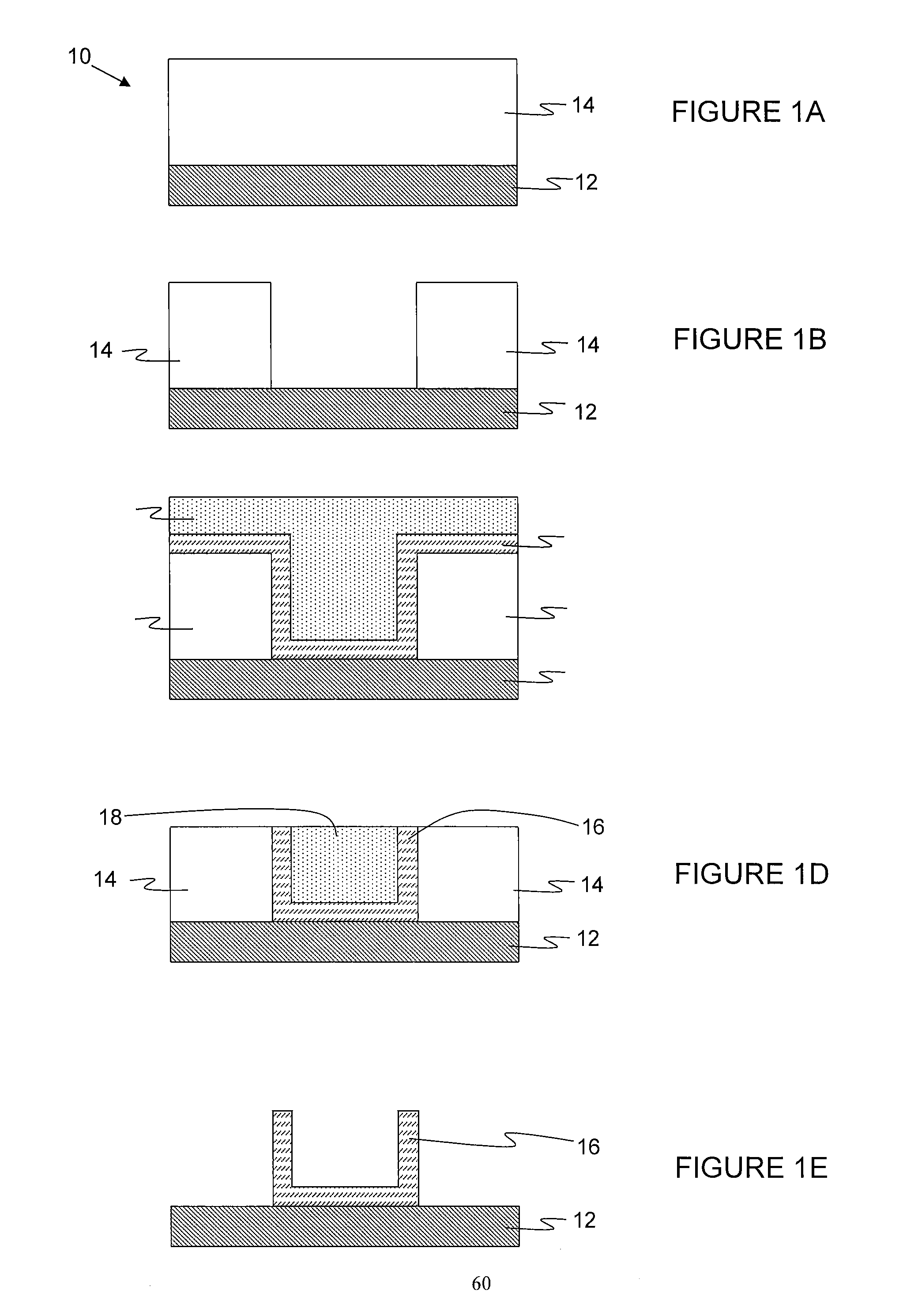
FIELD OF THE INVENTION[0001]The present invention relates to compositions for removing silicon-containing insulating layers from microelectronic devices, including vertical memory device structures, having same thereon.DESCRIPTION OF THE RELATED ART[0002]The semiconductor industry is driving toward smaller chip geometries and faster and more power-efficient memory devices. Advances in semiconductor processing and device design have resulted in chips with millions of circuit elements and interconnects. Today, memory devices implement hundreds of megabits of storage in a single integrated circuit. Such devices include volatile memory (e.g., dynamic random access memory (DRAM) and static random access memory (SRAM)), non-volatile memory (e.g., electrically erasable programmable read only memory (EEPROM), flash EEPROM, shallow trench isolation (STI), ferroelectric RAM and phase-change RAM), and combinations thereof. Memory performance is becoming increasingly important in determining th...
Claims
Login to View More Application Information
Patent Timeline
 Patent Type & AuthorityApplications(United States)
IPC IPC(8): C11D3/02C11D3/08C11D3/06C11D3/28C11D3/43C11D1/00
CPCC11D3/0073H01L27/10844C11D3/042C11D3/046C11D3/06C11D3/08C11D3/28C11D3/30C11D3/43C11D7/08C11D7/3209C11D7/3218C11D7/3281C11D7/5004C11D11/0047H01L21/02074H01L21/02101H01L21/31111C11D3/02H10B12/01C11D2111/22
InventorVISINTIN, PAMELA M.KORZENSKI, MICHAEL B.
OwnerADVANCED TECH MATERIALS INC