Gallium oxide single crystal composite, process for producing the same, and process for producing nitride semiconductor film utilizing gallium oxide single crystal composite

a technology of gallium oxide and composites, which is applied in the direction of crystal growth process, polycrystalline material growth, nanoinformatics, etc., can solve the problems of large lattice constant mismatch, interface reactivity, and high-frequency properties degradation, so as to reduce lattice mismatch, high quality, and low cost

Inactive Publication Date: 2009-03-19
NIPPON LIGHT METAL CO LTD +1
View PDF0 Cites 7 Cited by
  • Summary
  • Abstract
  • Description
  • Claims
  • Application Information

AI Technical Summary

Benefits of technology

[0038]The gallium oxide single crystal composite of the present invention has the gallium nitride layer formed of cubic gallium nitride on the surface of the gallium oxide single crystal. Thus, in the case where the gallium oxide single crystal composite is used as a nitride semiconductor substrate formed of a group III-V nitride semiconductor formed of gallium nitride (GaN), aluminum nitride (AlN), indium nitride (InN), a mixed crystal thereof, or the like, a high quality cubic nitride semiconductor film in which mixing of a hexagonal crystal can be reduced and a cubic crystal is grown dominantly over the hexagonal crystal can be obtained. The phrase “a cubic crystal is grown dominantly over the hexagonal crystal” indicates that abundance of the cubic crystal is higher than that of the hexagonal crystal. The gallium oxide single crystal composite of the present invention has the gallium nitride layer formed of cubic gallium nitride on its surface, to thereby reduce lattice mismatch at an interface with the substrate upon crystal growth of cubic gallium nitride (GaN) as much as possible and allow epitaxial growth of a high quality cubic GaN film, in particular.
[0039]The process for producing a gallium oxide single crystal composite of the present invention requires advantageous conditions compared with conditions required for obtaining a bulk gallium nitride single crystal, for example, and is advantageous in that the gallium oxide single crystal composite can be obtained at low cost because the gallium nitride layer formed of cubic gallium nitride can be formed on the surface of the gallium oxide single crystal by simple means and the gallium oxide single crystal available with relative ease is used.
[0040]The process for producing a nitride semiconductor film of the present invention provides the nitride semiconductor film by using the gallium oxide single crystal composite. Thus, the method can provide a high quality cubic nitride semiconductor film in which mixing of the hexagonal crystal can be reduced and the cubic crystal is grown dominantly over the hexagonal crystal. The gallium oxide single crystal composite may be used for epitaxial growth of the cubic nitride semiconductor without separately forming a buffer layer because the gallium oxide single crystal is provided with the gallium nitride layer formed of cubic gallium nitride on its surface, and a production process may be simplified.

Problems solved by technology

However, Si has merits of realizing a large diameter wafer and low cost, but has problems in degraded high-frequency properties, interface reactivity with GaN, and extensive mismatch in lattice constant with GaN.
Further, GaAs has better high-frequency properties than those of Si but extensive lattice mismatch as Si, and thus, a crystal of a device level is hardly formed.
In addition, As or P is not suitable as a material to be actively used hereafter in consideration of environmental problems.
For example, the cubic crystal gradually changes into the hexagonal crystal through partial etching of a GaAs substrate during an initial growth process due to heat decomposition of the GaAs substrate, to thereby lose interface smoothness, generate many stacking faults from a part without smoothness, and to increase the stacking faults.
In this way, a high quality cubic GaN thin film is hardly obtained on a crystal growth plane, and a quality of a cubic epitaxial film to be obtained is not sufficient compared with that of a hexagonal epitaxial film.
However, the bulk GaN single crystal has a large N2 vapor pressure and a high melting point during formation, so the bulk GaN single crystal substrate is hardly formed by a normal melting method.
Accordingly, there arise problems such as a complex crystal formation apparatus and high cost.
There are formation methods such as a liquid phase epitaxy (LPE) method and an Na flux method, but those methods each have difficulties in control of a crystal structure and therefore have problems in quality.

Method used


Image

  • Gallium oxide single crystal composite, process for producing the same, and process for producing nitride semiconductor film utilizing gallium oxide single crystal composite
  • Gallium oxide single crystal composite, process for producing the same, and process for producing nitride semiconductor film utilizing gallium oxide single crystal composite
  • Gallium oxide single crystal composite, process for producing the same, and process for producing nitride semiconductor film utilizing gallium oxide single crystal composite

Examples


example 1

Production of Gallium Oxide Single Crystal

[0052]First, gallium oxide powder having a purity of 99.99% was sealed in a rubber tube, and was molded into a rod at a gravitational pressure of 450 MPa. The resultant was placed in an electric furnace and fired at 1,600° C. for 20 hours in atmospheric air, to thereby obtain a gallium oxide sintered product. The rod obtained after firing had a size of about 9 mmΦ×40 mm.

[0053]Next, growth of a gallium oxide single crystal was performed by using this gallium oxide sintered product as a raw material rod by an optical floating zone (FZ) method. A double ellipsoid-type infrared heating furnace (SS-10W, manufactured by ASGAL Informatik GmbH) was used for growth of the single crystal.

[0054]To be specific, the gallium oxide sintered product obtained above was provided on an upper shaft as a raw material rod, and the gallium oxide single crystal was provided on a lower shaft as a seed crystal. A crystal growth atmosphere was a dry air atmosphere con...

example 2

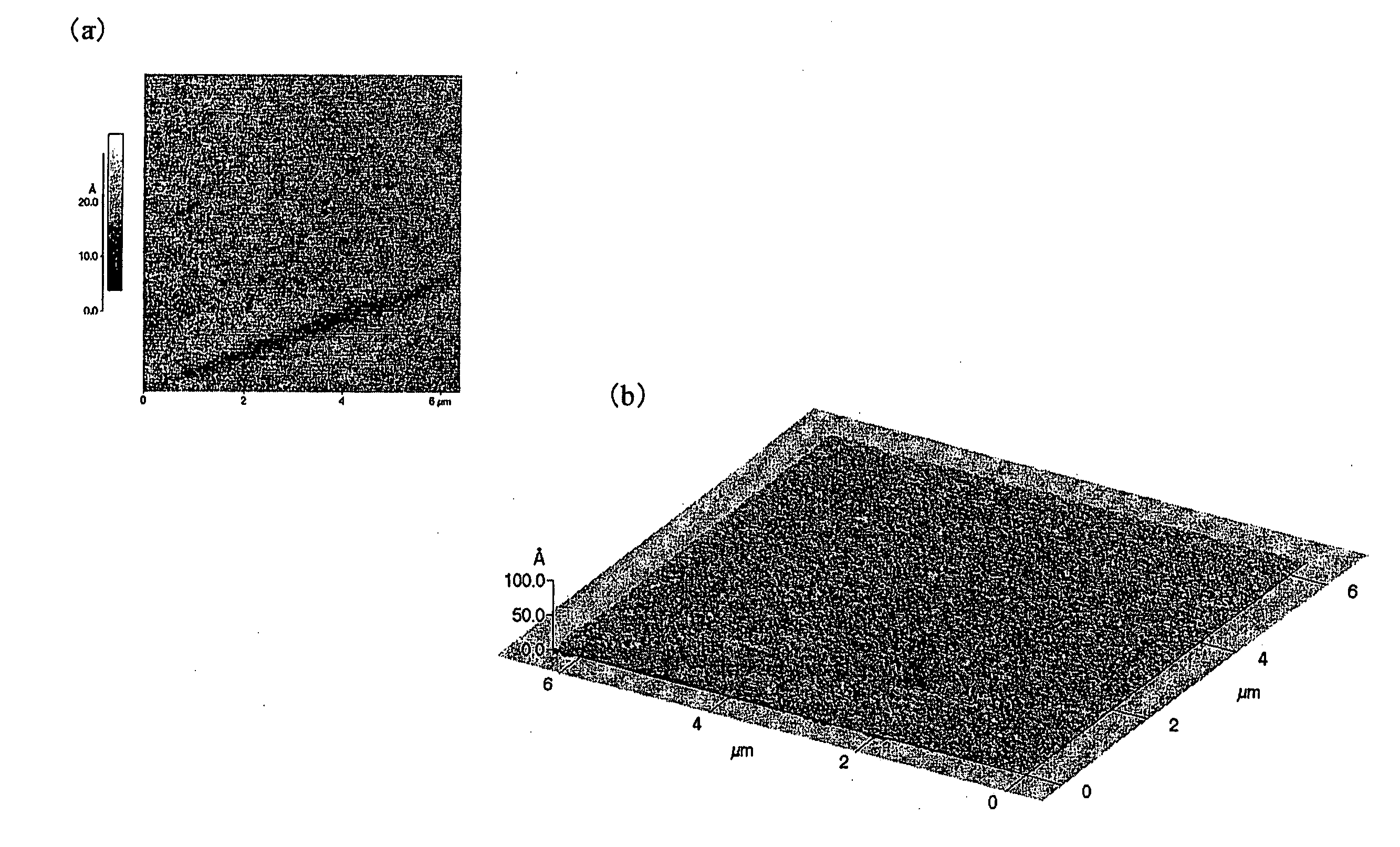
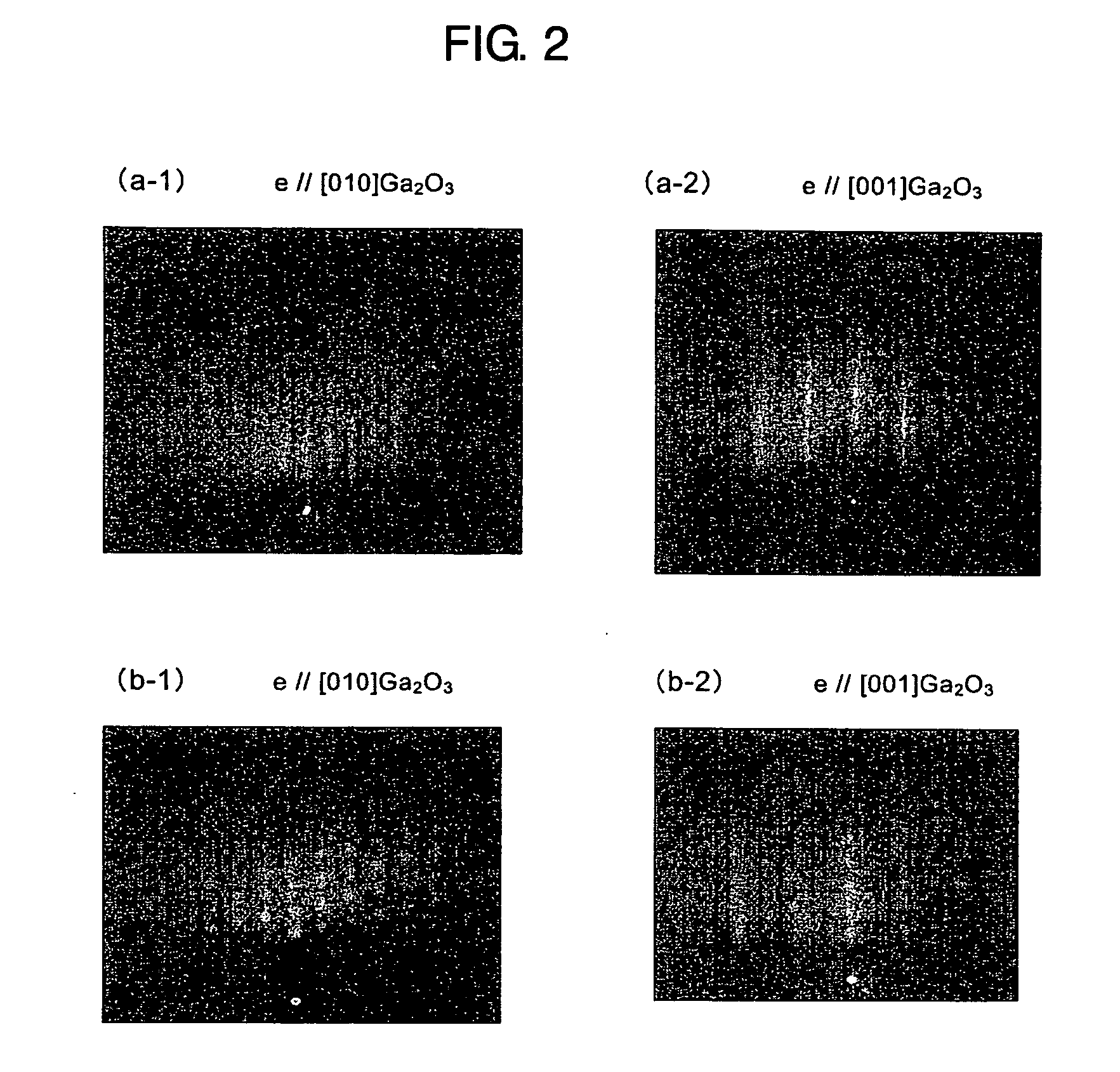
[0058]A gallium oxide single crystal was produced and cut out to a size of 8 mm length×8 mm width×2 mm thickness in the same manner as in Example 1. The (100) plane of the gallium oxide single crystal was subjected to polishing treatment through chemical mechanical polishing (CMP) employing colloidal silica. FIG. 2 shows reflection high-energy electron diffraction (RHEED) patterns of the surface of the CMP-treated gallium oxide single crystal. FIG. 2(a-1) shows an RHEED pattern obtained upon injection of an electron beam from a [010] direction of the gallium oxide single crystal, and FIG. 2(a-2) shows an RHEED pattern obtained upon injection of an electron beam from a [001] direction of the gallium oxide single crystal. For reference, FIG. 2(b) shows RHEED patterns of the case where the (100) plane of the gallium oxide single crystal was subjected to polishing treatment through hand polishing with SiC emery paper and buff. FIG. 2(b-1) shows an RHEED pattern obtained upon injection o...

example 3

Production of Gallium Nitride Film

[0062]The gallium oxide single crystal composite obtained in Example 1 was used for growth of a gallium nitride film.

[0063]The gallium oxide single crystal composite was set in an RF-MBE apparatus, and a gallium nitride film with a thickness of about 500 nm was grown on the surface of the gallium oxide single crystal composite by using a nitrogen (N2) gas as a nitrogen source and solid Ga as a Ga source under the conditions including a temperature (i.e., substrate temperature) of the gallium oxide single crystal composite of 880° C., a nitrogen gas flow rate of 2 sccm, an RF power of 330 W, and a film formation time of 60 min.

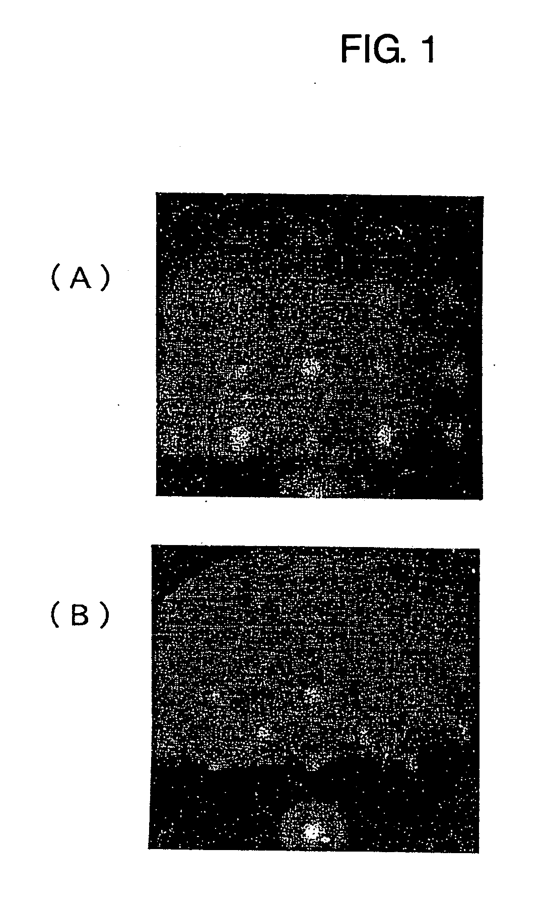
Reflection High-Energy Electron Diffraction

[0064]FIG. 5 shows reflection high-energy electron diffraction (RHEED) patterns of the surface of the gallium nitride film grown on the surface of the gallium oxide single crystal composite as described above. As shown in FIG. 5, two typical patterns of (A) and (B) were observed, and a...


PUM

PropertyMeasurementUnit
thicknessaaaaaaaaaa
thicknessaaaaaaaaaa
thicknessaaaaaaaaaa

Abstract

Provided are: a gallium oxide single crystal composite, which can provide, for example, upon a crystal growth of a nitride semiconductor, a high-quality cubic crystal in which mixing of a hexagonal crystal is reduced to thereby realize dominant growth of a cubic crystal over hexagonal crystal, and which can be utilized as a substrate particularly suitable for epitaxial growth of cubic GaN; a process for producing the same; and a process for producing a nitride semiconductor film. The gallium oxide single crystal composite has a gallium nitride layer formed of cubic gallium nitride on a surface of the gallium oxide single crystal; the process for producing the gallium oxide single crystal composite includes subjecting the surface of gallium oxide single crystal to nitriding treatment using ECR plasma or RF plasma to form the gallium nitride layer formed of cubic gallium nitride on the surface of the gallium oxide single crystal; and further, the process for producing the nitride semiconductor film includes growing the nitride semiconductor film on the surface of the gallium oxide single crystal composite by an RF-MBE method.

Description

TECHNICAL FIELD[0001]The present invention relates to a gallium oxide single crystal composite having a gallium nitride layer formed of cubic gallium nitride (GaN) on a surface of a gallium oxide (Ga2O3) single crystal, to a process for producing the gallium oxide single crystal composite, and to a process for producing a nitride semiconductor film using the gallium oxide single crystal composite. The gallium oxide single crystal composite can be used as a substrate used for forming a group III-V nitride semiconductor formed of gallium nitride (GaN), aluminum nitride (AlN), indium nitride (InN), a mixed crystal thereof, or the like, and is particularly preferably used for formation of cubic GaN.BACKGROUND ART[0002]A group III-V nitride semiconductor formed of gallium nitride (GaN), aluminum nitride (AlN), indium nitride (InN), a mixed crystal thereof, or the like is a direct transmission-type and may have a band gap capable of being designed from 0.7 eV to 6.2 eV. Thus, various appl...

Claims


Application Information

Patent Timeline
Patent Type & Authority Applications(United States)
IPC IPC(8): H01L29/205C30B23/02C30B29/38C30B29/16C30B29/40H01L21/20H01L21/203H01L21/205
CPCB82Y10/00B82Y30/00C30B23/02C30B29/16H01L21/02658H01L21/0242H01L21/0254H01L21/02631C30B29/406H01L21/20
Inventor OOHIRA, SHIGEONANISHI, YASUSHIARAKI, TSUTOMUYAMAGUCHI, TOMOHIRO
Owner NIPPON LIGHT METAL CO LTD
Why Eureka
Try Eureka