Process for producing oriented inorganic crystalline film, and semiconductor device using the oriented inorganic crystalline film

a technology of inorganic crystalline film and oriented inorganic crystalline film, which is applied in the direction of non-metal conductors, conductors, and gel states, can solve the problems of high equipment cost, use the technique disclosed, and waste of considerable amounts of materials, etc., and achieves low cost, low-cost manufacturing, and superior element characteristics.

Active Publication Date: 2009-06-18
FUJIFILM CORP
View PDF5 Cites 3990 Cited by
  • Summary
  • Abstract
  • Description
  • Claims
  • Application Information

AI Technical Summary

Benefits of technology

[0070]As explained above, the process for producing the oriented inorganic crystalline film 1 according to the first embodiment comprises the steps of: (A) forming on the substrate 11 the non-monocrystalline film 12 containing inorganic crystalline particles 20 by a liquid phase technique using a raw-material solution which contains a raw material and an organic solvent, where the inorganic crystalline particles 20 have a layered crystal structure and are contained in the raw material; and (B) crystallizing the non-monocrystalline film 12 by heating the non-monocrystalline film 12 to a temperature equal to or higher than the crystallization temperature of the non-monocrystalline film 12 so that part of the inorganic crystalline particles 20 act as crystal nuclei in the crystallization stage. In such a process, the orientation of the oriented inorganic crystalline film 1 can be controlled without utilizing the crystallinity or orientation of the layer underlying the non-monocrystalline film 12. Therefore, even when the underlying layer does not have orientation as an amorphous substrate, a randomly-oriented substrate, or the like, it is possible to form the inorganic crystalline film 1 so as to be oriented.
[0071]Thus, in the process according to the first embodiment, it is possible to form an oriented inorganic crystalline film immediately on an unoriented underlying layer such as an amorphous substrate (which is inexpensive) by using a liquid phase technique (which is simple and entails low cost).
[0072]In particular, the process according to the first embodiment enables simple, low-cost manufacturing, by a liquid phase technique, of an oriented semiconductor film which is preferable for use as an active layer

Problems solved by technology

However, the vacuum processes for the vacuum film formation and the photolithographic patterning are complex and entail high equipment cost.
In addition, since unnecessary portions of uniformly formed films are removed, considerable amounts of materials are wasted.
Nevertheless, since the organic semiconductors tend to be inferior to the inorganic semiconductors in performance and durability, it is desirable

Method used


Image

  • Process for producing oriented inorganic crystalline film, and semiconductor device using the oriented inorganic crystalline film
  • Process for producing oriented inorganic crystalline film, and semiconductor device using the oriented inorganic crystalline film

Examples


example 1

4.1 Concrete Example 1

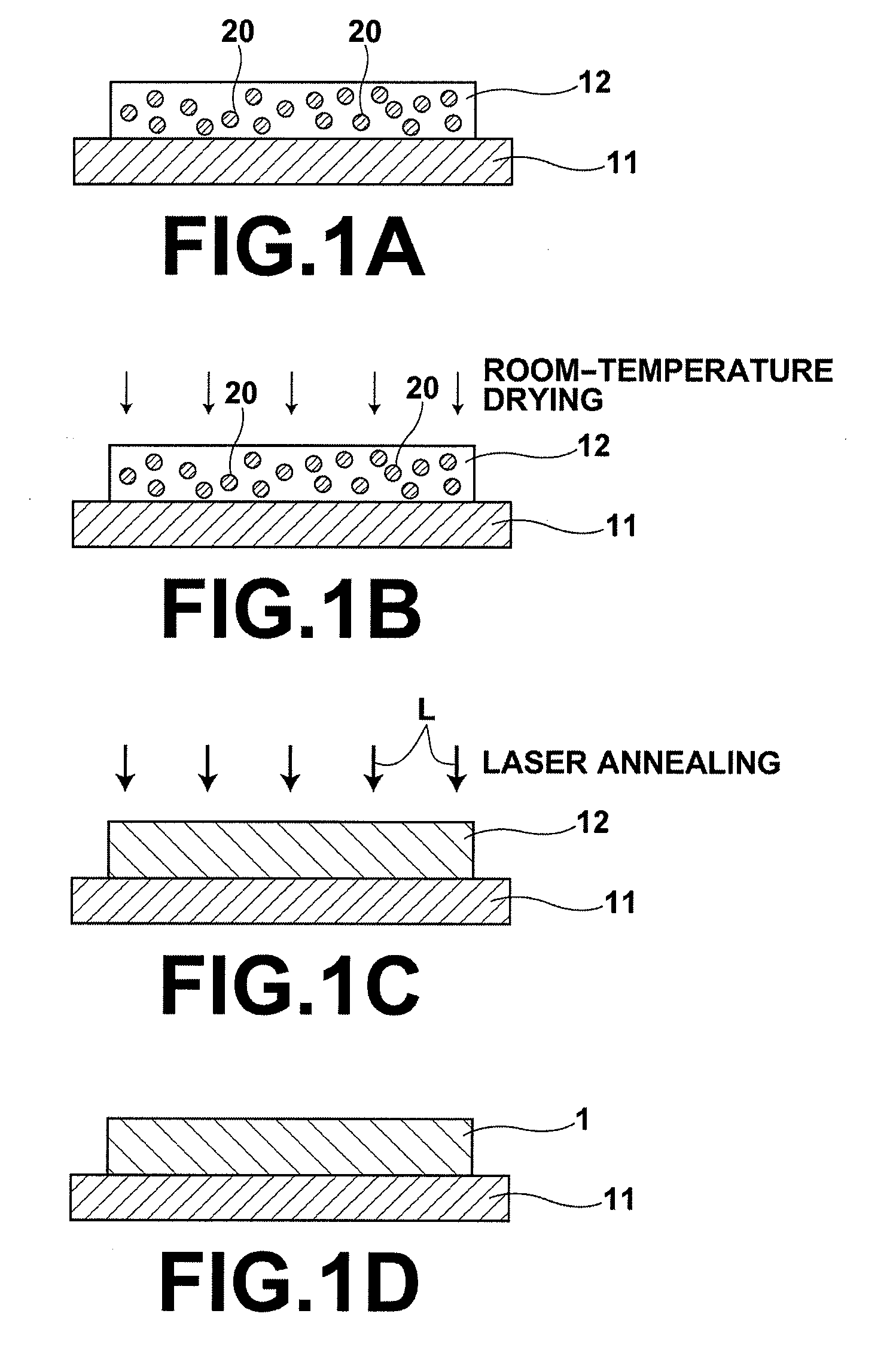
[0083]The concrete example 1 of the oriented inorganic crystalline film according to the present invention has been produced as follows.

[0084]First, a film of ZnxGayInzO(x+3y / 2+3z / 2−d) (which is hereinafter referred to as IGZO) has been formed by using crystalline nanoparticles of IGZO, which have been produced by a sol-gel process, where x, y, and z are real numbers greater than zero, and satisfy the relationship,

0≦d≦(x+3y / 2+3z / 2) / 10.

[0085]A raw-material solution to be applied to a substrate has been prepared as follows. A solution having a light-yellow color (hereinafter referred to as the solution A) has been prepared by mixing 2.2 g of zinc acetate dihydrate, 2.47 g of gallium isopropoxide, and 2.74 g of indium isopropoxide into cyclohexanol and stirring the mixture at 150° C. The relative composition (the ratio between molar fractions) In:Ga:Zn of the solution B has been measured as 1.08:1:1 by ICP (inductively coupled plasma) spectroscopy. Then, a solutio...

example 2

4.4 Concrete Example 2

[0094]The concrete example 2 of the oriented inorganic (IGZO) crystalline film according to the present invention is different from the concrete example 1 in that the non-monocrystalline film has been crystallized by laser annealing. In the laser annealing, the non-monocrystalline film has been irradiated with the KrF excimer laser light having the wavelength of 248 nm, the laser irradiation power has been controlled by use of an attenuator, and the number of laser shots has been 200. The most superior crystallinity has been obtained when the laser irradiation power is 103 mJ / cm2.

[0095]The IGZO film crystallized as above has been analyzed by XRD. The greatest X-ray diffraction intensity has been observed at the diffraction angle 2θ of 30.8 degrees, which corresponds to the (009) face, and the normalized X-ray diffraction peak intensity at the diffraction angle 2θ of 55.7 degrees corresponding to the (110) face (i.e., the I value) of the crystallized non-monocry...

example 3

4.5 Concrete Example 3

[0097]The concrete example 3 of the oriented inorganic (IGZO) crystalline film according to the present invention is different from the concrete example 1 in that the solution B is prepared by heating and stirring the solution A at 230° C. (instead of 250° C.) for an hour, and the non-monocrystalline film has been crystallized by laser annealing with the KrF excimer laser light (as the concrete example 2).

[0098]The solution B prepared as above has a russet color. After the solution B has been prepared, the relative composition (the ratio between molar fractions) In:Ga:Zn has been measured as 1.05:1:1, and the average diameter of the crystalline nanoparticles dispersed in the solution B has been measured to be approximately 5 nm.

[0099]Thereafter, a non-monocrystalline IGZO film has been formed in a similar manner to the concrete example 1, and crystallized by laser annealing in a similar manner to the concrete example 2. Specifically, the non-monocrystalline fil...


PUM


Abstract

In a process for producing an oriented inorganic crystalline film, a non-monocrystalline film containing inorganic crystalline particles is formed on a substrate by a liquid phase technique using a raw-material solution which contains a raw material and an organic solvent, where the inorganic crystalline particles have a layered crystal structure and are contained in the raw material. Then, the non-monocrystalline film is crystallized by heating the non-monocrystalline film to a temperature equal to or higher than the crystallization temperature of the non-monocrystalline film so that part of the inorganic crystalline particles act as crystal nuclei.

Description

BACKGROUND OF THE INVENTION[0001]1. Field of the Invention[0002]The present invention relates to a process for producing an oriented inorganic crystalline film having a layered crystal structure, and the oriented inorganic crystalline film. In addition, the present invention also relates to a semiconductor device (such as a thin-film transistor (TFT)) using the oriented inorganic crystalline film.[0003]2. Description of the Related Art[0004]Recently, various flexible devices have been receiving attention. The use of the flexible devices is widely spread, and the flexible devices include, for example, electronic paper, flexible displays, and the like.[0005]Conventionally, the flexible devices, as well as the devices using glass substrates, are mainly manufactured by vacuum film formation (such as sputtering or vacuum evaporation) and photolithographic patterning. However, the vacuum processes for the vacuum film formation and the photolithographic patterning are complex and entail hi...

Claims


Application Information

Patent Timeline
IPC IPC(8): H01B1/00H01L21/20
CPCC30B1/02C30B29/22H01L21/02422H01L29/7869H01L21/02565H01L21/02628H01L21/02554
Inventor UMEDA, KENICHIHIRAI, HIROYUKITANAKA, ATSUSHIKOHDA, KATSUHIROHIGASHI, KOHEISUNAGAWA, HIROSHI
Owner FUJIFILM CORP
Why Eureka
Try Eureka