
Method of Manufacturing High Quality ZnO Monocrystal Film on Silicon(111) Substrate

a monocrystal film, widebandgap technology, applied in the direction of single crystal growth, polycrystalline material growth, chemistry apparatus and processes, etc., can solve the problems of inability to apply the homoepitaxial growth technology of zno monocrystal film to the industry, and it is more difficult to prepare a p-n junction zno-based device, etc., to achieve excellent photoelectronic performance

Inactive Publication Date: 2009-11-26
THE CHINESE ACADEMY OF SCI THE INST OF PHYSICS
View PDF3 Cites 8 Cited by
  • Summary
  • Abstract
  • Description
  • Claims
  • Application Information

AI Technical Summary

Benefits of technology

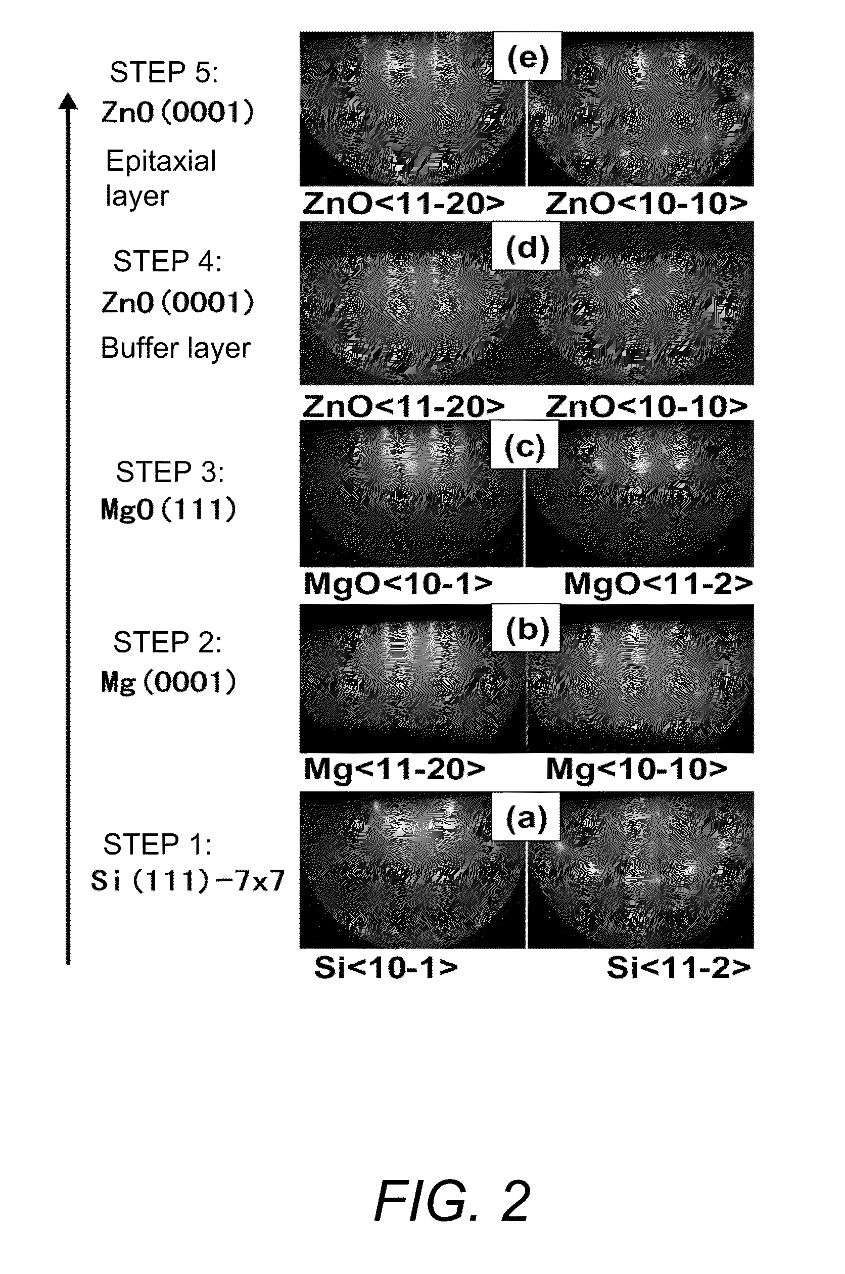
[0014]The difference between the above-mentioned method of manufacturing the ZnO monocrystal film and the prior art method lies mainly in that depositing the monocrystal film of metal Mg at low temperature to protect the clean Si (111) surface, and obtaining the magnesium oxide monocrystal film by means of the active oxygen treatment at low temperature. Being at low temperature aims to prevent a silicification reaction between Si and Mg through mutual diffusion, which may influence the interface between Si and Mg; moreover, depositing Mg at low temperature may decrease the desorption speed of Mg, so as to obtain a stable monocrystal layer. We found the obvious mutual diffusion between Si and Mg above 60° C., whereby an Mg2Si layer is formed as a result. We clearly observed the related patterns of Mg2Si (111) with RHEED (Reflection High Energy Electron Diffraction), which indicates that there is Mg2Si formed on Si. However, there is apparently less mutual diffusion through the interface below 30° C., which may allow to obtain the high crystalline Mg monocrystal film, which has been proved by the clear RHEED patterns of Mg (0001). After the low-temperature Mg monocrystal film is formed, an active oxygen source is introduced, such as oxygen-contained RF plasma, ECR (Electron Cyclotron Resonance) plasma or ozone. The active oxygen diffuses toward the Mg film, thus gradually oxidizing the Mg film into the monocrystal magnesium oxide. Since the formation enthalpy Hf (MgO) of MgO is much smaller than the formation enthalpy Hf (SiO2) of SiO2, it is difficult for Si to combine with oxygen, which thus protects the surface of Si. The RHEED patterns indicate that the high-quality halite-phase MgO monocrystal layer can be obtained by this method, which thus provides a good template for the epitaxial growth of ZnO. We obtained the high-quality ZnO monocrystal film by the two-step method.
[0016]The above-mentioned method of manufacturing the ZnO monocrystal film by protecting the surface of Si substrate through depositing Ca at low temperature is different from that through depositing Mg at low temperature mainly in that, the deposition temperature and the oxidation temperature of metal Ca are lower than those of Mg. This is because Ca is more active than Mg, and thus easier to react with Si to produce calcium silicide (CaSix). We discovered in our research that, we could not obtain the metal Ca monocrystal film when the temperature is above 0° C. because of the reaction between Si and Ca. Therefore, lower temperature is needed for the deposition of Ca. Similarly, the oxidization temperature of Ca is lower, too. Ca has a cubic close-packed structure with a lattice constant of 0.559 nm, the lattice mismatch between Ca and Si (a=0.543 nm) is only 2.8%, and thus it is easy to prepare a high-quality film. Moreover, the halite-phase calcium oxide has a lattice constant of 0.481 nm, the lattice in its (111) face is just between Si (111) and ZnO (0001) and closer to ZnO (the lattice mismatch is 4.5%), which is very suitable for the growth of ZnO.
[0018]Sr is more active, thus the above-mentioned deposition temperature of Sr is lower than that of Ca and Mg, and oxygen gas can be used instead of active oxygen to oxidize metal Sr, which is more convenient for operation. Sr has a cubic close-packed structure with a lattice constant of 0.608 nm, the lattice mismatch between Sr and Si (a=0.543 nm) is 12%, and thus a high-quality Sr film can be obtained. Moreover, the halite-phase strontium oxide has a lattice constant of 0.516 nm, the lattice in its (111) face is between Si (111) and ZnO (0001), which is also suitable for the growth of ZnO.
[0020]Cd is the least active among the four metal elements, therefore the above-mentioned deposition temperature of Cd is also the highest, and meanwhile active oxygen is needed to oxidize metal Cd. Being similar to Mg, Cd has a hexagonal close-packed crystal structure, with a lattice constant of 0.298 nm. Therefore, there is a domain-matching growth mode of 4:3 for the face of Cd (0001) and the face of Si (111), that is, 4 lattices of Cd match with 3 lattices of Si, with the lattice mismatch being only 3%. Therefore, the high-quality Cd film can be obtained. Moreover, the halite-phase cadmium oxide has a lattice constant of 0.471 nm, the lattice in its (111) face is between Si (111) and ZnO (0001) and closer to ZnO (the lattice mismatch is 2.5%), which is very suitable for the growth of ZnO.

Problems solved by technology

Although a ZnO monocrystal substrate has been commercialized, it is still too expensive.
Therefore, the homoepitaxial growth technology of the ZnO monocrystal film cannot currently be applied to industry.
However, the insulated sapphire substrate makes it more difficult to prepare a p-n junction ZnO-based device.
However, there are currently few reports in the world about epitaxial growth of the ZnO film, especially the high-quality ZnO monocrystal film, on the Si substrate.
One of the important reasons is that Si is easy to form amorphous-structured silicon oxide (SiOx) in an oxygen environment, which thus makes the ZnO epitaxial growth very difficult At present, some surface and interface treatment technologies have been developed at domestically and abroad to protect the silicon surface, and thus the ZnO film has been prepared.

Method used


Image

  • Method of Manufacturing High Quality ZnO Monocrystal Film on Silicon(111) Substrate
  • Method of Manufacturing High Quality ZnO Monocrystal Film on Silicon(111) Substrate
  • Method of Manufacturing High Quality ZnO Monocrystal Film on Silicon(111) Substrate

Examples


embodiment 1

Preparation of the High-Quality ZnO Thin Film by Predepositing the Metal Mg Monocrystal Thin Layer on Si (111)

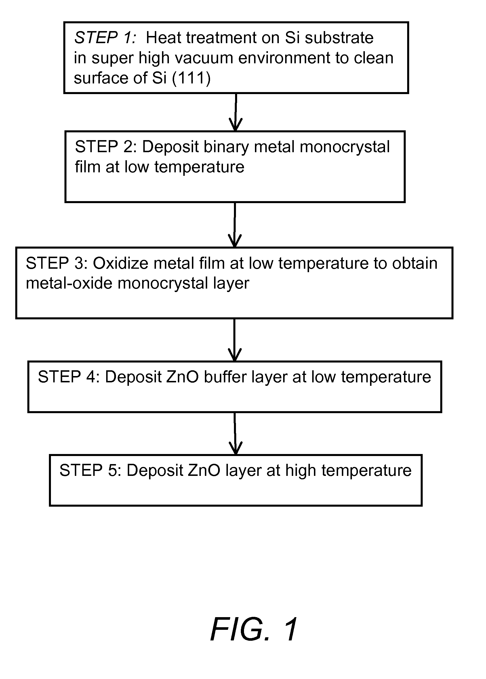
[0029]In the process flow chart of the invention as shown in FIG. 1, the high-quality ZnO thin film can be prepared by predepositing the metal Mg monocrystal thin layer on the substrate of Si (111), with the specific steps as follows:[0030]1. Remove the silicon oxide layer on the surface of commercially available Si (111) substrate by means of the publicly-known hydrofluoric acid corrosion method, and introduce the substrate into the MBE system;[0031]2. raise the temperature to 900° C. at atmospheric pressure below 5.0×10⁻⁷ Pa and keep for 20 minutes, so as to remove the remaining silicon oxide layer on the surface of Si by high-temperature desorption, and obtain the clean surface of Si substrate;[0032]3. cool the Si substrate to −10° C., and here its surface shows typical (7×7) reconstruction; heat an Mg diffusion furnace to make the Mg beam reach 8×10⁻⁵ Pa; and deposit the...

embodiment 2

Preparation of the High-Quality ZnO Thin Film by Predepositing the Metal Mg Monocrystal Thin Layer on Si (111)

[0036]In the process flow chart of the invention as shown in FIG. 1, the high-quality ZnO thin film can be prepared by predepositing the metal Mg monocrystal thin layer on the substrate of Si (111), with the specific steps as follows:[0037]1. Remove the silicon oxide layer on the surface of commercially available Si (111) substrate by means of the publicly-known hydrofluoric acid corrosion method, and introduce the substrate into the MBE system;[0038]2. raise the temperature to 900° C. at atmospheric pressure below 5.0×10⁻⁷ Pa and keep for 20 minutes, so as to remove the remaining silicon oxide layer on the surface of Si by high-temperature desorption, and obtain the clean surface of Si substrate;[0039]3. cool the Si substrate to 30° C., and here its surface shows typical (7×7) reconstruction; heat the Mg diffusion furnace to make the Mg beam reach 8×10⁻⁵ Pa, and deposit the...

embodiment 3

Preparation of the High-Quality ZnO Thin Film by Predepositing the Metal Mg Monocrystal Thin Layer on Si (111)

[0043]In the process flow chart of the invention as shown in FIG. 1, the high-quality ZnO thin film can be prepared by predepositing the metal Mg monocrystal thin layer on the substrate of Si (111), with the specific steps as follows:[0044]1. Remove the silicon oxide layer on the surface of commercially available Si (111) substrate by means of the publicly-known hydrofluoric acid corrosion method, and introduce the substrate into the MBE system;[0045]2. raise the temperature to 900° C. at atmospheric pressure below 5.0×10⁻⁷ Pa and keep for 20 minutes, so as to remove the remaining silicon oxide layer on the surface of Si by high-temperature desorption, and obtain the clean surface of Si substrate;[0046]3. cool the Si substrate to −30° C., and here its surface shows typical (7×7) reconstruction; heat the Mg diffusion furnace to make the Mg beam reach 8×10⁻⁵ Pa; and deposit th...


PUM


Abstract

There is provided a method of manufacturing high quality ZnO manufacturing film on silicon (111) substrate, including the following steps: removing silicon oxide on the surface of silicon (111) substrate; depositing metal monocrystal film having 1-10 nm thickness, such as Mg, Ca, Sr, Cd etc, at low temperature; oxiding the metal film at low temperature to obstain metal oxide monocrystal layer; depositing ZnO buffer layer at low temperature; depositing ZnO epitaxial layer at high temperature. The ZnO film is suitable for fabrication of high performance of photoelectron device.

Description

FIELD OF THE INVENTION[0001]The present invention relates to a method of manufacturing a wide-bandgap semiconductor zinc oxide (ZnO) monocrystal film.BACKGROUND OF THE INVENTION[0002]As a core basic material of the third generation semiconductor, ZnO has excellent photoelectronic performance, with the bandgap width at room temperature being 3.37 eV and the free exciton binding energy 60 meV. It has become another important wide bandgap semiconductor material after GaN (with the free exciton binding energy of 25 meV), and has a wide application prospect in manufacturing high-performance short-wavelength photoelectronic devices. Its application in devices is based on manufacturing a device quality ZnO-based epitaxial film. Although a ZnO monocrystal substrate has been commercialized, it is still too expensive. Therefore, the homoepitaxial growth technology of the ZnO monocrystal film cannot currently be applied to industry. Similar to the case of GaN, sapphire is a common substrate fo...

Claims


Application Information

Patent Timeline
IPC IPC(8): H01L21/20
CPCC30B23/02C30B29/16H01L21/02381H01L21/02433H01L21/02439H01L21/02658H01L21/02516H01L21/02554H01L21/02609H01L21/02614H01L21/02488
Inventor DU, XIAOLONGWANG, XINAZENG, ZHAOQUANYUAN, HONGTAOMEI, ZENGXIAXUE, QIKUNJIA, JINFENG
Owner THE CHINESE ACADEMY OF SCI THE INST OF PHYSICS
Learn More