Flexible Circuit Assemblies without Solder and Methods for their Manufacture

a flexible circuit and assembly technology, applied in the field of electronic assembly, can solve the problems of high toxic substances, dangerous fumes produced by soldering operations, and potential hazards for workers, and achieve the effects of reducing costs and complexity, shortening manufacturing cycle time, and reducing reliability problems of pcb

Active Publication Date: 2010-04-22
FJELSTAD JOSEPH CHARLES
View PDF16 Cites 35 Cited by
  • Summary
  • Abstract
  • Description
  • Claims
  • Application Information

AI Technical Summary

Benefits of technology

[0020]The assembly, built with a novel reverse-interconnection process (RIP), uses no solder, thus bypassing the use of lead, tin, and heat associated problems. The term “reverse” refers to the reverse order of assembly; components are placed first and then circuit layers manufactured rather than creating a PCB first and then mounting components. No conventional PCB is required (although one may be optionally integrated), shortening manufacturing cycle time, reducing costs and complexity, and lessening PCB reliability problems.
[0021]RIP products are robust with respect to mechanical shock and thermal cycle fatigue failure. In comparison to conventional products placed on PCB boards, components incorporated into RIP products require no standoff from the surface and thus have a lower profile and can more densely spaced. Moreover, because no solderable finish is required and fewer materials and fewer process steps are required, RIP products are lower-cost. In addition, RIP products are amenable to in-place thermal enhancements (including improved heat dissipation materials and methods) that also may provide integral electromagnetic interference (EMI) shielding. Moreover the structure may be assembled with embedded electrical and optical components.

Problems solved by technology

Lead is a highly toxic substance, exposure to which can produce a wide range of well known adverse health effects.
Of importance in this context, fumes produced from soldering operations are dangerous to workers.
Each of these constituents has been shown to be potentially hazardous.
Mining lead can contaminate local ground water supplies.
Smelting can lead to factory, worker, and environmental contamination.
Because of the difficulty and cost of recycling used electronics, as well as lax enforcement of legislation regarding waste exports, large amounts of used electronics are sent to countries such as China, India, and Kenya, which have lower environmental standards and poorer working conditions.
Thus, there are marketing and legislative pressures to reduce tin / lead solders.
RoHS does not eliminate the use of lead in all electronic devices.
SAC solders also have significant environmental consequences.
For example, mining tin is disastrous both locally and globally.
Perhaps the most serious environmental impact of mining tin in Brazil is the silting up of rivers and creeks.
This degradation modifies forever the profile of animal and plant life, destroys gene banks, alters the soil structure, introduces pests and diseases, and creates an irrecoverable ecological loss.
These range from pressures on global warming from the destruction of rain forest to the long term damage to the pharmaceutical industry by the destruction of animal and plant life diversity.
SAC solders have additional problems.
They require high temperatures, wasting energy, are brittle, and cause reliability problems.
The melting temperature is such that components and circuit boards may be damaged.
Moreover, SAC solder processes are prone to the formation of shorts (e.g., “tin whiskers”) and opens if surfaces are not properly prepared.
Therefore there is a need for a substitute for the soldering process and its attendant environmental and practical drawbacks.
While such solutions offer benefits in specific applications, the input / output (I / O) terminals of the chip can be very small and very challenging to make such connections accurately.
Moreover the device after manufacturing may not successfully pass burn in testing making the entire effort valueless after completion.
Another area of concern is in management of heat as densely packaged ICs may create a high energy density that can reduce the reliability of electronic products.

Method used


Image

  • Flexible Circuit Assemblies without Solder and Methods for their Manufacture
  • Flexible Circuit Assemblies without Solder and Methods for their Manufacture
  • Flexible Circuit Assemblies without Solder and Methods for their Manufacture

Examples


Embodiment Construction

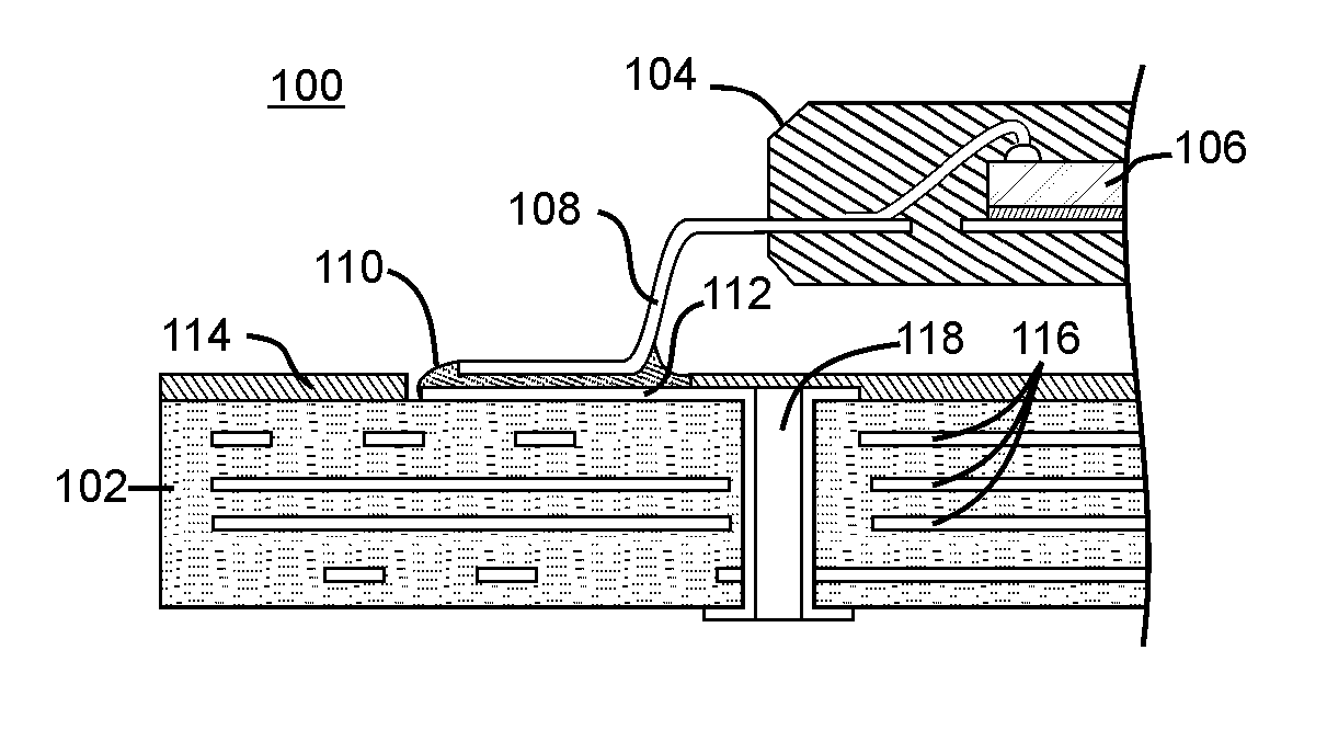
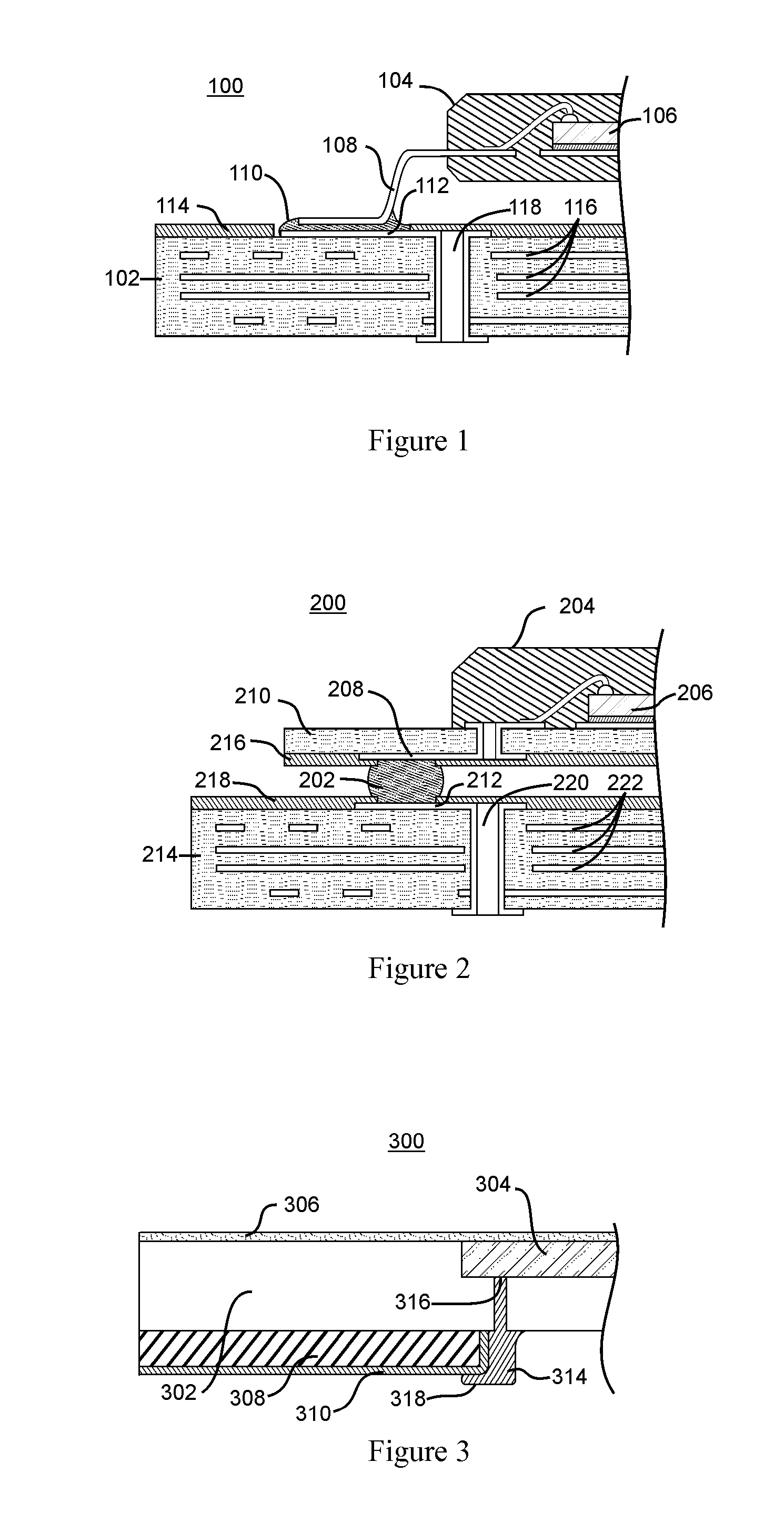
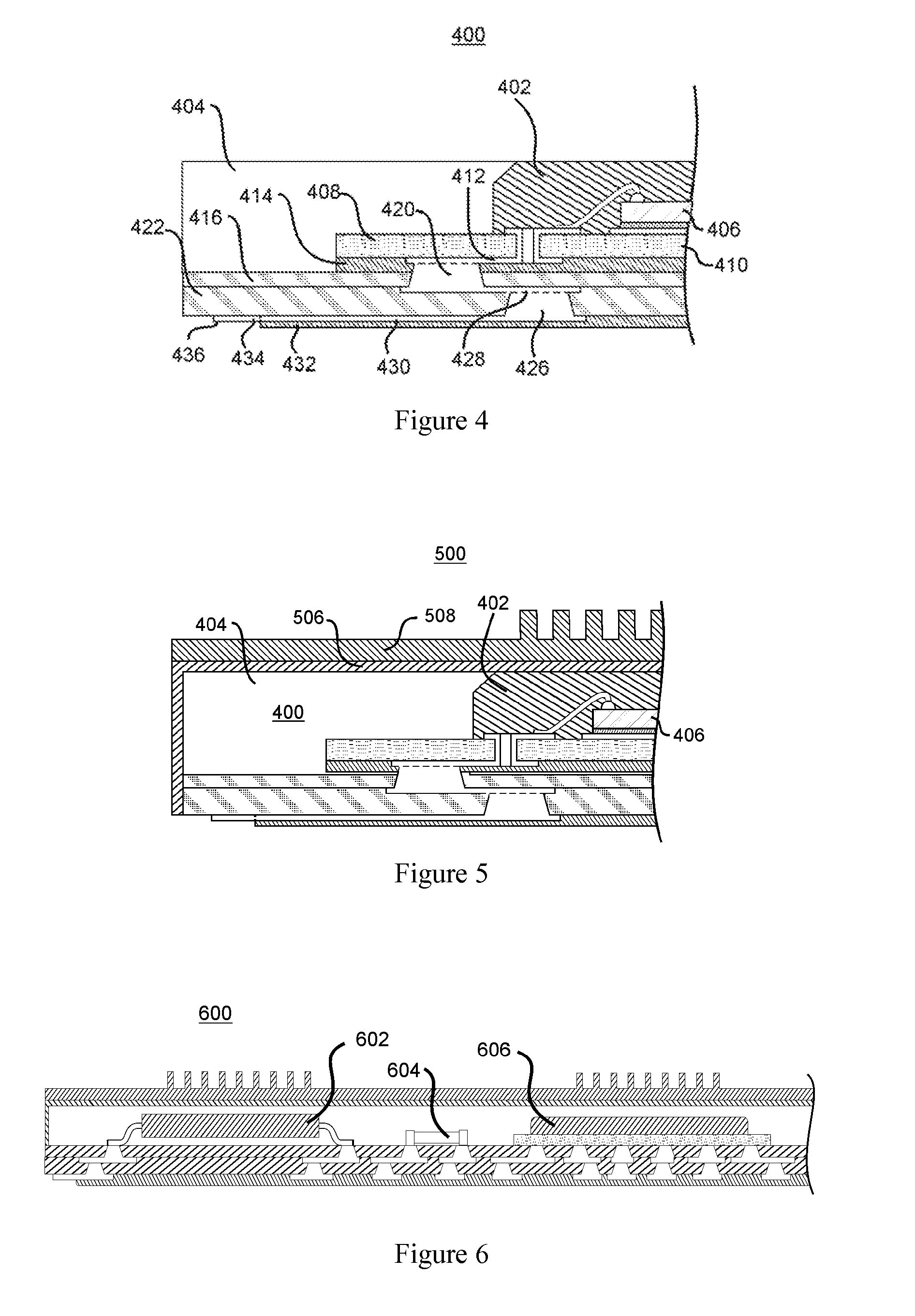
[0082]In the following description and in the accompanying drawings, specific terminology and drawing symbols are set forth to provide a thorough understanding of the present invention. In some instances, the terminology and symbols may imply specific details that are not required to practice the invention. For example, the interconnection between conductor elements of components (i.e., component I / O leads including electro-optical ports) may be shown or described as having multi-conductors interconnecting to a single lead or a single conductor signal line connected to multiple component contacts within or between devices. Thus each of the multi-conductor interconnections may alternatively be a single-conductor signaling, control, power or ground line and vice versa. Circuit paths shown or described as being single-ended may also be differential, and vice-versa. The interconnected assembly may be comprised of standard interconnections; microstrip or stripline interconnections and al...


PUM

PropertyMeasurementUnit
flexibleaaaaaaaaaa
electrically insulatingaaaaaaaaaa
electrically conductiveaaaaaaaaaa

Abstract

The present invention provides an electronic assembly 400 and a method for its manufacture 800, 900, 1000 1200, 1400, 1500, and 1700. The assembly 400 uses no solder. Components 406 or component packages 402, 802, 804, 806 with I/O leads 412 are placed 800 onto a planar substrate 808. The assembly is encapsulated 900 with electrically insulating material 908 with vias 420, 1002 formed or drilled 1000 through the substrate 808 to the components' leads 412. Then the assembly is plated 1200 and the encapsulation and drilling process 1500 repeated to build up desired layers 422, 1502, 1702. The planar substrate 808 may be a flexible substrate 2016 allowing bending of an assembly 2000 to fit into various enclosures.

Description

CROSS REFERENCE TO RELATED APPLICATIONS[0001]This application claims the benefit of and priority to “FLEXIBLE CIRCUIT ASSEMBLIES WITHOUT SOLDER AND METHODS FOR THEIR MANUFACTURE,” U.S. Application No. 61 / 106,398 filed on Oct. 17, 2008, hereby incorporated by reference in its entirety.[0002]This application claims the benefit of PCT Application No. PCT / U.S.08 / 63123 filed on May 8, 2008 which claimed priority to: “ELECTRONIC ASSEMBLY WITHOUT SOLDER,” U.S. Application No. 60 / 928,467, filed on May 8, 2007; “ELECTRONIC ASSEMBLY WITHOUT SOLDER AND METHODS FOR THEIR MANUFACTURE,” U.S. Application No. 60 / 932,200, filed on May 29, 2007; “SOLDERLESS FLEXIBLE ELECTRONIC ASSEMBLIES AND METHODS FOR THEIR MANUFACTURE,” U.S. Application No. 60 / 958,385, filed on Jul. 5, 2007; “ELECTRONIC ASSEMBLIES WITHOUT SOLDER AND METHODS FOR THEIR MANUFACTURE,” U.S. Application No. 60 / 959,148, filed on Jul. 10, 2007; “MASS ASSEMBLY OF ENCAPULSATED ELECTRONIC COMPONENTS TO A PRINTED CIRCUIT BOARD BY MEANS OF AN ...

Claims


Application Information

Patent Timeline
Patent Type & Authority Applications(United States)
IPC IPC(8): H05K1/00B32B38/04B32B37/00
CPCH01L24/31Y10T156/1057H01L2224/48227H01L2224/48247H01L2224/48465H01L2924/01013H01L2924/01029H01L2924/01078H01L2924/01079H01L2924/14H01L2924/15311H01L2924/3025H05K1/189H05K3/284H05K3/32H05K2201/09481H05K2203/1316H05K2203/1469H01L24/48Y10T156/10H01L2924/12041H01L2224/73265H01L2224/32245H01L2924/00H01L2924/3512H01L21/568H01L2924/1815H01L2924/181H01L2924/00014H01L2924/00012H01L2224/45099H01L2224/45015H01L2924/207
Inventor FJELSTAD, JOSEPH C.
Owner FJELSTAD JOSEPH CHARLES
Why Eureka
Try Eureka