Driver circuit and display device

a technology of drive circuit and display device, which is applied in the direction of electrical apparatus casing/cabinet/drawer, pulse technique, instruments, etc., can solve the problems of deterioration of oxide semiconductor over time, increase of manufacturing cost, and remained variation of threshold voltage due to oxide semiconductor deterioration

Active Publication Date: 2010-05-06
SEMICON ENERGY LAB CO LTD
View PDF100 Cites 90 Cited by
  • Summary
  • Abstract
  • Description
  • Claims
  • Application Information

AI Technical Summary

Benefits of technology

[0010]According to one embodiment of present invention, a shift of a threshold voltage of a thin film transistor and an off current can be reduced without enlargement of an area occupied by circuits.

Problems solved by technology

If the number of gate lines and source lines is increased, there is a problem that a manufacturing cost is increased because it comes to be difficult to mount an IC chip including a driver circuit for driving the gate line and the source line by bonding or the like.
However, a unipolar driver circuit formed using amorphous silicon has a problem about a shift of threshold voltage with deterioration of the thin film transistor.
Further, the unipolar driver circuit formed using polysilicon has a problem that variations in the threshold voltage become apparent.
On the other hand, when a unipolar driver circuit is provided with a thin film transistor using an oxide semiconductor, although the problem of a shift of the threshold voltage and variations in the threshold voltage are not as apparent as in the case of the driver circuit having a thin film transistor formed using amorphous silicon or polysilicon, the problem that variations in the threshold voltage due to deterioration of the oxide semiconductor over time is remained.

Method used


Image

  • Driver circuit and display device
  • Driver circuit and display device
  • Driver circuit and display device

Examples


embodiment 1

[0042]In this embodiment, an n-channel thin film transistor is used as a thin film transistor including an oxide semiconductor which forms a unipolar driver circuit. An advantage of one mode of the present invention is to be described by giving an example of a source line driver circuit and / or a gate line driver circuit as a driver circuit for driving a pixel portion.

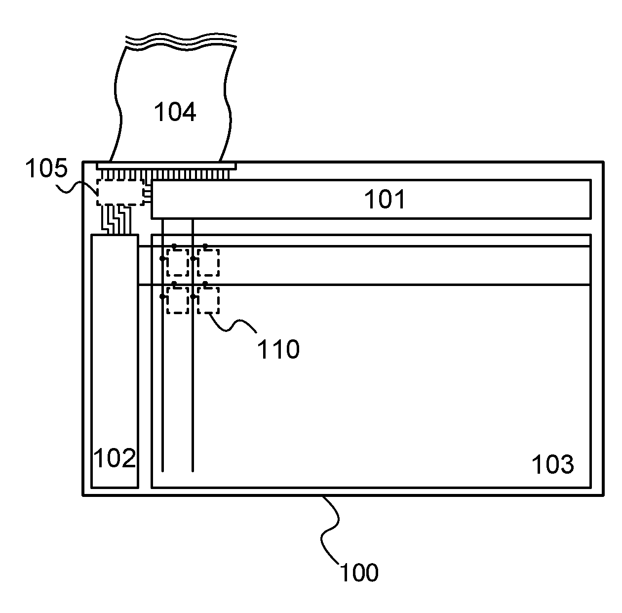
[0043]First, FIG. 1 shows an overall schematic view of a display device. A source line driver circuit 101, a gate line driver circuit 102, and a pixel portion 103 are integrally formed over a substrate 100. In the pixel portion 103, a portion surrounded by a dotted flame 110 is one pixel. Although an example in FIG. 1 shows a structure in which the gate line driver circuit 102 is provided for one end portion, a structure including a plurality of gate driver circuits 102 may be applied. Further, in a pixel of a display device, a thin film transistor (hereinafter referred to as a TFT) controls a display element. A signal ...

embodiment 2

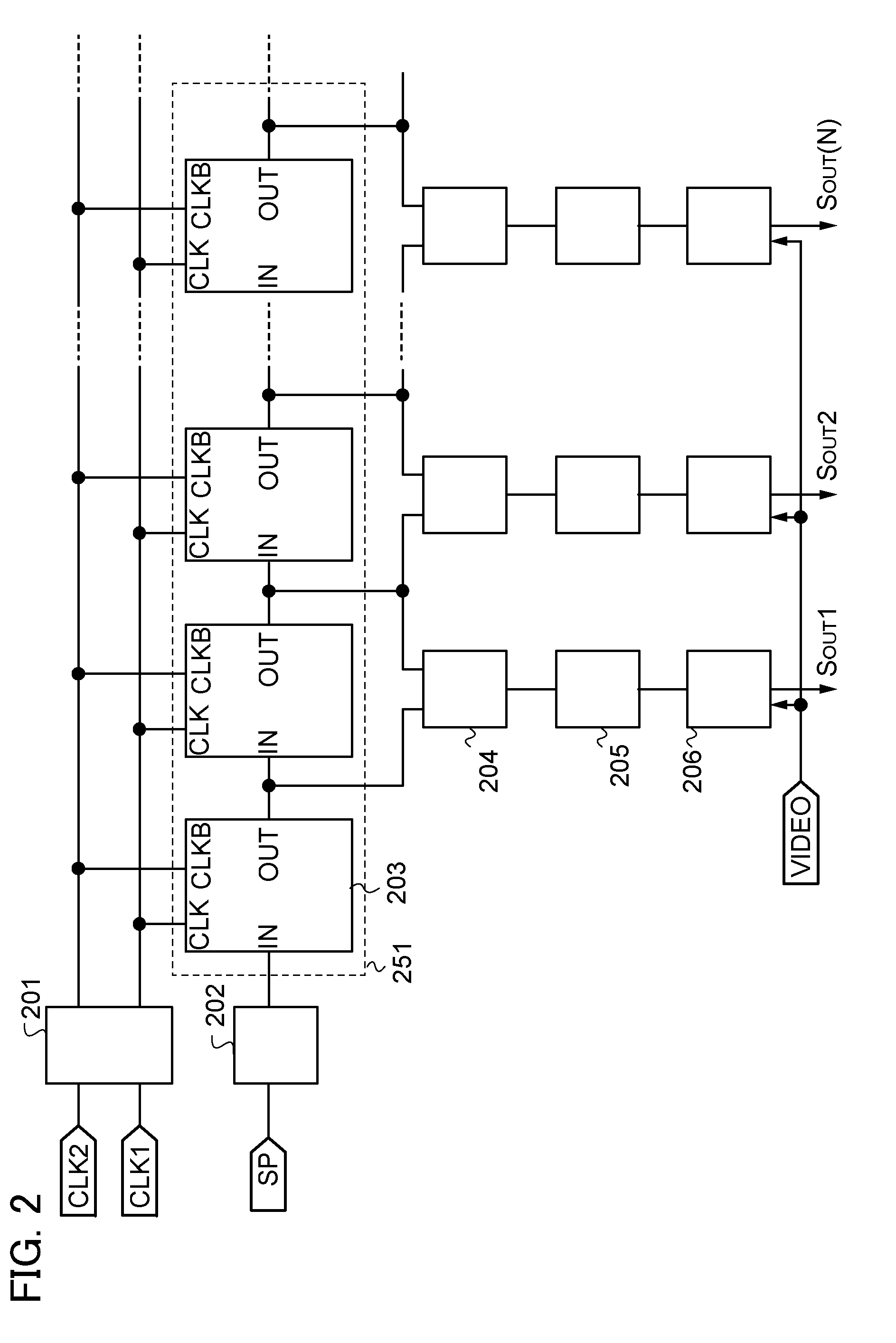
[0146]The above embodiment shows an example of a shift register of a static circuit as a shift register in a driver circuit of a display device. In this embodiment, an example of a driver circuit including a shift register of a dynamic circuit is described.

[0147]A structure of a pulse output circuit included in a shift register of a dynamic circuit is described with reference to FIGS. 14A to 14D. A pulse output circuit 1400 shown in FIG. 14A, as an example, includes an inverter circuit 1401 in which a start pulse SP is input from an input terminal, a switch 1402 of which one of terminals is connected to an output terminal of the inverter circuit 1401, and a capacitor 1403 connected to the other terminal of the switch 1402. Note that on / off of the switch 1402 in a pulse output circuit in an odd-numbered stage is controlled by the first clock signal (CLK1). On / off of the switch 1402 in a pulse output circuit in an even-numbered stage is controlled by the second clock signal (CLK2).

[01...

embodiment 3

[0157]In this embodiment, a manufacturing process of a display device including a driver circuit is described with reference to FIGS. 16A to 16C, FIGS. 17A to 17C, FIG. 18, FIG. 19, FIG. 20, FIG. 21, FIGS. 22A to 22D, and FIG. 23.

[0158]In FIG. 16A, for a light-transmitting substrate 1600, a glass substrate of barium borosilicate glass, aluminoborosilicate glass, or the like can be used.

[0159]Next, after a conductive layer is formed over the entire surface of the substrate 1600, a first photolithography step is performed to form a resist mask, and an unnecessary portion is removed by etching, whereby wirings and an electrode (a gate wiring including a gate electrode layer 1601 of a pixel TFT portion, a capacitor wiring 1608 of a capacitor portion, and a first terminal 1621 of a terminal portion) are formed. At this time, the etching is performed so that at least an end portion of the gate electrode layer 1601 is tapered. A cross-sectional view of this step is shown in FIG. 16A. Note ...


PUM


Abstract

The driver circuit includes an inverter circuit having a first thin film transistor including a first oxide semiconductor film and a second transistor including a second oxide semiconductor film. The first thin film transistor and the second thin film transistor are enhancement transistors, in which a silicon oxide film including an OH group is provided on and in contact with the first oxide semiconductor film and the second oxide semiconductor film, and a silicon nitride film is provided on and in contact with the silicon oxide film.

Description

TECHNICAL FIELD[0001]The present invention relates to a driver circuit using an oxide semiconductor, a manufacturing method thereof, a display device provided with the driver circuit, and an electronic device provided with the display device.BACKGROUND ART[0002]As typified by a liquid crystal display device, a thin film transistor formed over a flat board such as a glass substrate, is formed of amorphous silicon or polycrystalline silicon. A thin film transistor formed using amorphous silicon can cope with the increase of the glass substrate size even though electric field effect mobility is low. On the other hand, since a crystallization process such as laser annealing is needed, a thin film transistor formed using polycrystalline silicon does not always cope with the increase of the glass substrate size even though electric field effect mobility is high.[0003]Accordingly, a technique of manufacturing a thin film transistor by using an oxide semiconductor and applying the thin film...

Claims


Application Information

Patent Timeline
Patent Type & Authority Applications(United States)
IPC IPC(8): H05K7/00H03B1/00G09G5/00
CPCH01L27/1248H01L27/1225H01L27/1214
Inventor KOYAMA, JUNYAMAZAKI, SHUNPEI
Owner SEMICON ENERGY LAB CO LTD
Why Eureka
Try Eureka