

Perylene-imide semiconductor polymers
a technology of peryleneimide and semiconductors, applied in the field of peryleneimide semiconductor polymers, can solve the problems of poor processability and/or negligible electron mobilities of ambient conditions in n-channel polymers of otfts to date, and achieve excellent charge transport characteristics, high performance, and large solubility
- Summary
- Abstract
- Description
- Claims
- Application Information
AI Technical Summary
Benefits of technology
Problems solved by technology
Method used
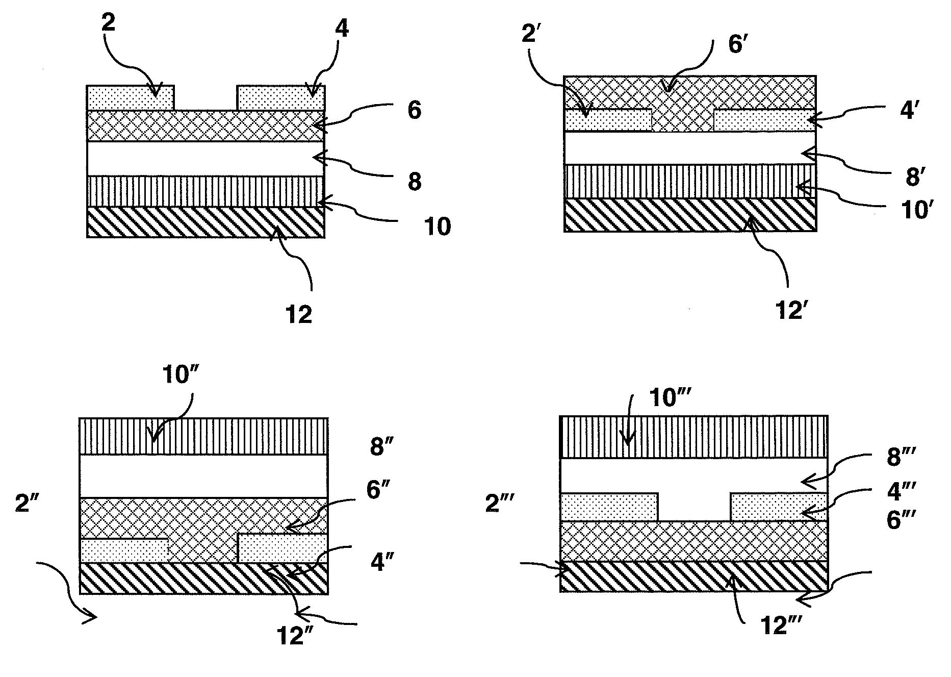
Image

Examples
example 1
Preparation of poly{[N,N′-bis(2-octyldodecyl)-3,4:9,10-perylene diimide-(1,7 & 1,6)-diyl]-alt-5,5′-(2,2′-bithiophene)} [P(PDI2OD-T2)]
Preparation of N,N′-bis(2-octyldodecyl)-(1,7 & 1,6)-dibromoperylene-3,4:9,10-bis(dicarboxiamide) (PDI2OD-Br2)
[0154]A mixture of PDA-Br2 (0.44 g, 0.80 mmol), 2-octyldodecylamine (0.71 g, 2.4 mmol), o-xylene (3 mL), and propionic acid (1 mL) was stirred at 140° C. for 2 h. Upon cooling to room temperature, most of solvents were removed in vacuo, and the residue was purified by column chromatography on silica gel with a mixture of chloroform:hexane (1:1, v / v, slowly up to 2:1) as eluent, affording a red solid as the product (0.63 g, 0.57 mmol, yield 71.5%). 1H NMR (CDCl3 500 MHz): δ: 9.51 (d, J=8.0 Hz, 2H), 8.94 (s, 2H), 8.71 (d, J=8.0 Hz, 2H), 4.15 (d, J=7.0 Hz, 4H), 2.01 (m, 2H), 1.20-1.50 (m, 64H), 0.84-0.89 (m, 12H). Elemental Analysis (calc. C, 69.30; H, 8.00; N, 2.53): found C, 69.42; H, 8.13; N, 2.61.
Preparation of poly{{N,N′-bis(2-octyldodecyl)-3...
example 2
Preparation of poly{[N,N′-bis(2-octyldodecyl)-3,4:9,10-perylene diimide-(1,7 & 1,6)-diyl]-alt-5,5′-(2,2′-bithiazole)} [P(PDI2OD-TZ2)]
[0157]Under argon, a mixture of PDI2OD-Br2 (123.8 mg, 0.112 mmol), 5,5′-bis(trimethylstannyl)-2,2′-bithiazole (55.1 mg, 0.112 mmol), and Pd(PPh3)2Cl2 (2.4 mg, 0.003 mmol) in anhydrous toluene (7 mL) was stirred at 90° C. for 1 day.
[0158](0.3 mL) was then added and the resulting mixture was stirred for an additional 12 hours. After cooling to room temperature, a solution of potassium fluoride (1 g) in water (2 mL) was added. This mixture was stirred and shaken at room temperature for 1 hour, before it was diluted with chloroform (150 mL). The resulting mixture was washed with water (100 mL×3), dried over anhydrous Na2SO4, and concentrated on a rotary evaporator. The residue was taken with chloroform (25 mL) and precipitated in methanol (50 mL). This procedure was repeated using chloroform and acetone, leading to a dark solid as the crude pro...
example 3
Electrochemistry, Optical Absorption, and MO Energies Determination
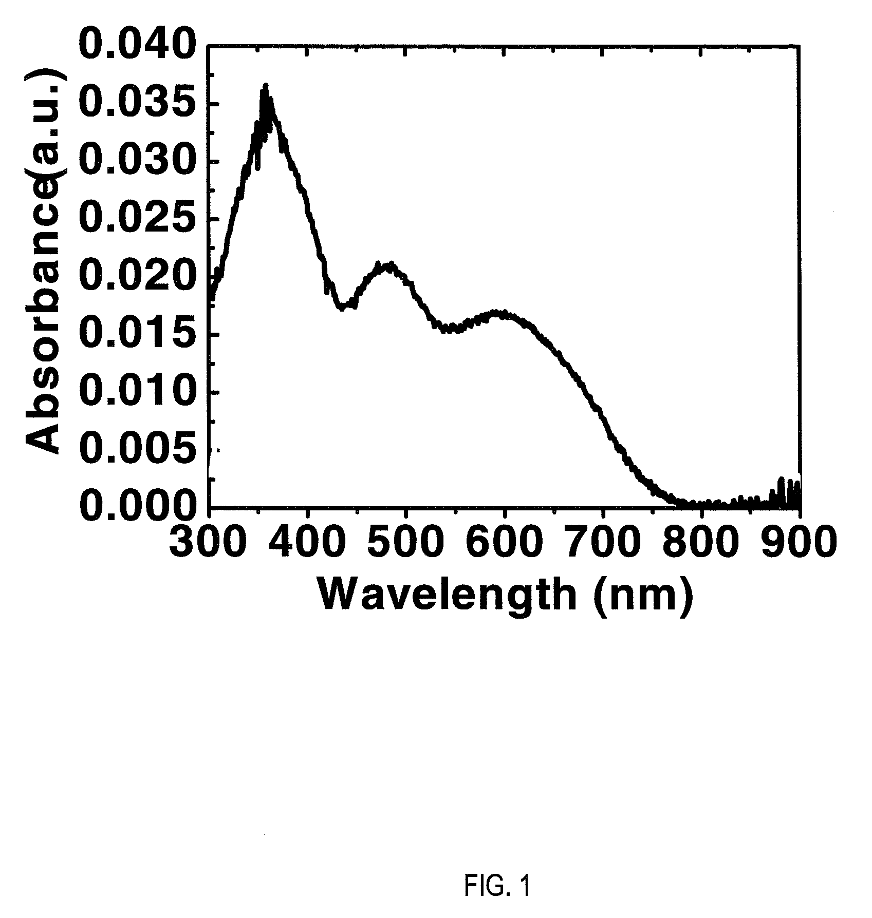
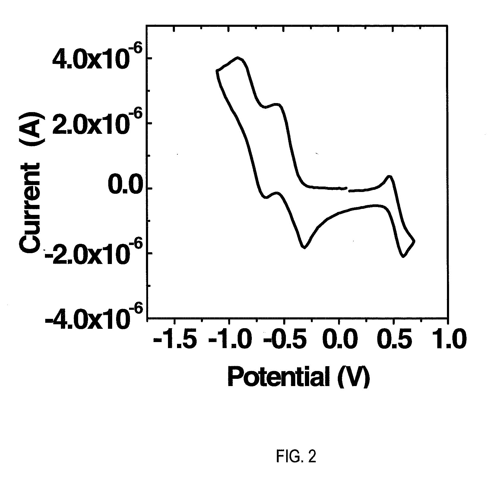
[0159]Electrochemical measurements were performed using a CH Instruments Model 660A electrochemical workstation. The solvent was dry tetrahydrofuran (THF) containing 0.1 M tetra-n-butylammonium hexaftuorophosphate electrolyte. A 1.0 mm diameter platinum disk electrode, a platinum wire counter electrode, and a Ag / AgxO reference electrode were employed. Ferrocene / Ferrocinium (Fc / Fc+, 0.54 V vs. SCE) was used as an internal reference for all measurements. Optical absorption spectra were obtained on thin films (˜30 nm on glass) with a Cary 1 Ultraviolet / Visible Spectrometer. ELUMO is calculated as:—(E1 / 2red-1+4.44 eV) assuming that Koopmans' theorem holds (EAred≈−ELUMO). SCE energy level is taken to be −4.44 eV below the vacuum level. EHOMO is calculated from: HOMO=LUMO−Eg (estimated from optical absorption spectra).
[0160]The optical absorption spectrum of P(PDI2OD-T2) exhibited three main absorptions located at λmax=594...
PUM
| Property | Measurement | Unit |
|---|---|---|
| viscosity | aaaaa | aaaaa |
| semiconductor | aaaaa | aaaaa |
| dielectric | aaaaa | aaaaa |
Abstract
Description
Claims
Application Information