Semiconductor light-emitting element, method for manufacturing the semiconductor light-emitting element and lamp that uses the semiconductor light-emitting element

a technology of semiconductor light-emitting elements and semiconductor light-emitting elements, which is applied in the direction of semiconductor/solid-state device manufacturing, semiconductor devices, electrical devices, etc., can solve the problems of difficult to fine film, reduce the adhesion of film to the underneath substrate, and block the light-emitting layer by the electrode, etc., to achieve excellent light-emitting properties, improve light permeability, and improve the effect of light permeability

Inactive Publication Date: 2011-03-17
SUMITOMO METAL MINING CO LTD
View PDF11 Cites 11 Cited by
  • Summary
  • Abstract
  • Description
  • Claims
  • Application Information

AI Technical Summary

Benefits of technology

[0037]The semiconductor light-emitting element of the present invention uses a transparent conductive film that is formed from an oxide of indium and gallium or an oxide of indium, gallium and tin as a transparent electrode that is provided on a p-type semiconductor layer, and annealed at a relatively low temperature of 200° C. to 480° C.
[0038]The transparent conductive film has transmittance of 85% or greater in the wavelength range near 450 nm, and a transmittance of 80% or greater in a wavelength range near 400 nm. Therefore, the transparent electrode of the semiconductor element of the present invention has better light permeability in both the blue range and ultraviolet range than a conventional transparent electrode that uses IZO film. In this way, the semiconductor light-emitting element of the invention has higher output of blue and ultraviolet light than a conventional semiconductor light-emitting element, and thus can be said to have excellent light-emitting properties.
[0039]In addition, the annealing process in order to obtain this effect, is performed in a temperature range of 200° C. to 480° C., which is lower than the temperature range of 500° C. to 900° C. that is required for IZO film, so there is no hindrance of the lowering of the specific resistance and contact resistance due to the gallium element in the p-type semiconductor layer diffusing into the transparent conductive film caused by high-temperature annealing. Therefore, by using this transparent conductive film, a transparent electrode having excellent light-emitting properties of blue and ultraviolet light, as well as low resistance can be obtained.
[0040]Furthermore, at the time that the transparent conductive film is formed on the p-type semiconductor layer, the film is amorphous, so etchability is excellent, and highly precise patterning is possible.

Problems solved by technology

In a gallium nitride semiconductor light-emitting element, current diffusion is small in the transverse direction, so current only flows into the semiconductor directly below the electrode, and when the electrode is not transparent, there is a problem in that the light that is emitted by the light-emitting layer is blocked by the electrode and cannot be obtained externally.
There are problems in that due to this mixing of films, over etching or insufficient etching such as the occurrence of etching residue may occur, and it may become difficult to make the film finer.
However, when water or hydrogen is added during film formation, problems occur in that the adherence of the film to the underneath substrate decreases, or the ITO target surface used is reduced and a large amount of nodules are generated, causing abnormal discharge such as arching.
Therefore, when ITO is used for an electrode of a light-emitting element that emits light having a wavelength in the ultraviolet range, there is a problem in that the output of emitted light is low.
However, as disclosed in patent literature 2, when performing this kind of annealing process at high temperature, it was found that problems occurred in that there is element interdiffusion near the boundary between the conductive oxide film and p-type semiconductor layer, which not only impedes the reduction of the specific resistance of the conductive oxide film, but is also linked to an increase in specific resistance of a p-type semiconductor layer and an increase in contact resistance between the conductive oxide film and p-type semiconductor layer.
On the other hand, amorphous IZO film that is not crystallized by an annealing process, has disadvantages in that the transmittance on the visible short-wavelength side with a wavelength of 400 to 450 nm, or in other words, the transmittance of blue light is low.Patent Literature 1: JP 2007-287845 A1Patent Literature 2: JP 2007-294578 A1Non-patent Literature: “Transparent Conductive Film Technology (Revision 2)”, Ohmsha, Ltd., Dec. 20, 2006, p.

Method used


Image

  • Semiconductor light-emitting element, method for manufacturing the semiconductor light-emitting element and lamp that uses the semiconductor light-emitting element
  • Semiconductor light-emitting element, method for manufacturing the semiconductor light-emitting element and lamp that uses the semiconductor light-emitting element
  • Semiconductor light-emitting element, method for manufacturing the semiconductor light-emitting element and lamp that uses the semiconductor light-emitting element

Examples


example 1

Manufacturing a Gallium Nitride Semiconductor Layer

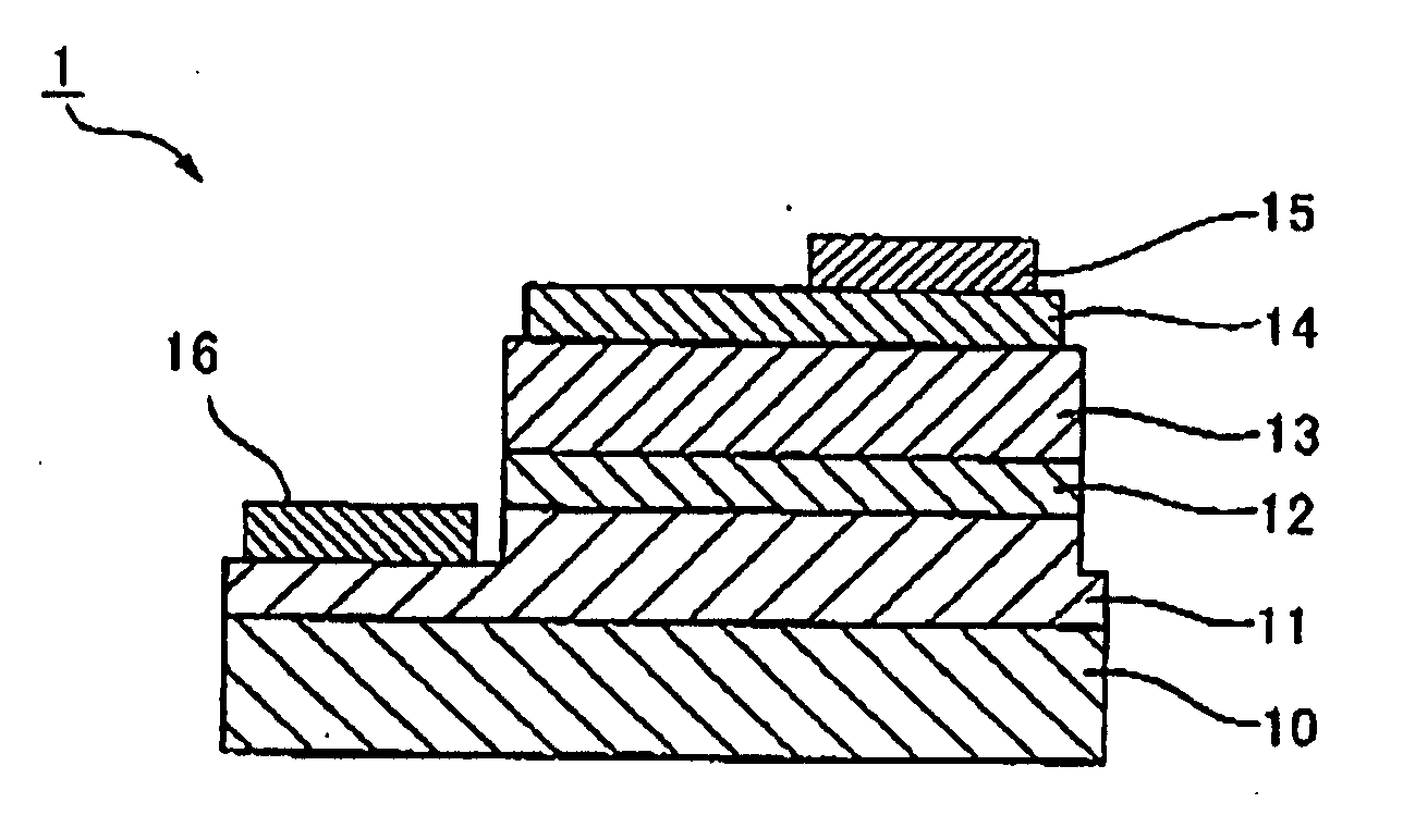
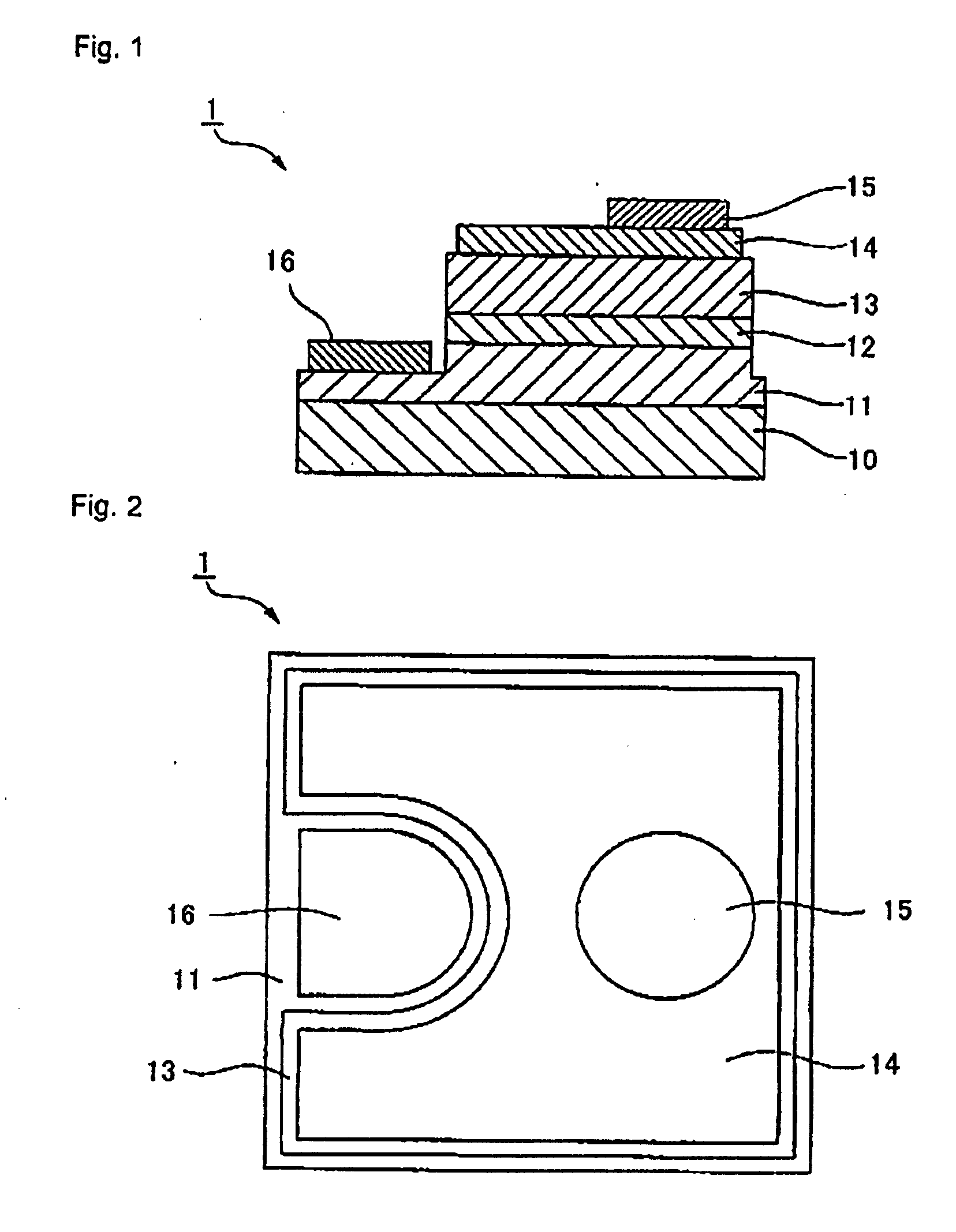
[0127]A gallium nitride semiconductor layer was manufactured as described below.

[0128]That is, an undoped GaN under layer (layer thickness 2000 nm), Si doped n-type GaN contact layer (layer thickness 2000 nm, carrier density=1×1019 cm−3), Si doped n-type Al0.07Ga0.93N clad layer (layer thickness 12.5 nm, carrier density=1×1018 cm−3), a multiple quantum structure comprising six Si doped GAN barrier layers (layer thickness 14.0 nm, carrier density=1×1018 cm−3) and five undoped In0.20Ga0.80N well layers (layer thickness 2.5 nm), Mg doped p-type Al0.07Ga0.93N clad layer (layer thickness 10 nm), and Mg doped p-type GaN contact layer (layer thickness 100 nm) were sequentially layered on a sapphire c-plane ((0001) crystal plane) substrate via an AlN buffer layer. Each of the layers of the layered structure of the gallium nitride semiconductor layer described was grown by reduced pressure MOCVD.

(Manufacturing the Semiconductor Light-Emittin...

example 2

[0139]The same semiconductor light-emitting element as in example 1 was manufactured except that the transparent conductive film that is formed on the p-type GaN contact layer of the gallium nitride semiconductor layer was changed to a transparent conductive film comprising an oxide of indium, gallium and tin, the annealing temperature after patterning of the transparent conductive film was 400° C., and after creating a vacuum of 1 Pa or less inside the furnace before the annealing process, highly pure nitrogen gas having a purity of 4N was introduced into the furnace.

[0140]Here, in the sputtering of the transparent conductive film, an oxide sintered compact target was used in which gallium was contained at an amount of a Ga / (In+Ga+Sn) atomic ratio of 0.15, and tin was contained at an amount of a Sn / (In+Ga+Sn) atomic ratio of 0.05.

[0141]The transparent conductive film (hereafter referred to as “GITO15”) comprising an oxide of indium, gallium and tin and formed by the method describe...

example 3

[0144]The same semiconductor light-emitting element as in example 1 was manufactured except that the transparent conductive film that is formed on the p-type GaN contact layer of the gallium nitride semiconductor layer was changed to a transparent conductive film comprising an oxide of indium, gallium and tin, the atmosphere of the annealing process after patterning of the semiconductor conductive film was a vacuum, and the annealing temperature was 400° C.

[0145]Here, in the sputtering of the transparent conductive film, an oxide sintered compact target was used in which gallium was contained at an amount of a Ga / (In+Ga+Sn) atomic ratio of 0.05, and tin was contained at an amount of a Sn / (In+Ga+Sn) atomic ratio of 0.09.

[0146]The transparent conductive film (hereafter referred to as “GITO5”) comprising an oxide of indium, gallium and tin and formed by the method described above, had relatively high transmittance of 85% or greater in the wavelength range of 450 nm and 75% or greater i...


PUM


Abstract

Provided are a semiconductor light-emitting element that is capable of efficiently outputting blue color or ultraviolet light, and a lamp using the semiconductor light-emitting element.
The semiconductor light-emitting element is obtained by a manufacturing method that, when manufacturing the semiconductor light-emitting element that comprises a compound semiconductor layer that includes at least a p-type semiconductor layer, and a transparent electrode that is provided on the p-type semiconductor layer, includes a step of forming a film comprising an oxide of indium and gallium, or forming a film comprising an oxide of indium, gallium and tin, in an amorphous state on the p-type semiconductor layer, so as to form a transparent conductive film, followed by a step of performing an annealing process on the transparent conductive film at a temperature of 200° C. to 480° C.

Description

TECHNICAL FIELD[0001]The present invention relates to a semiconductor light-emitting element, and particularly to a semiconductor light-emitting element that has excellent light-emitting output (Po) of ultraviolet light. Moreover, the present invention relates to a method for manufacturing the semiconductor light-emitting element, and a lamp that uses the semiconductor light-emitting element.RELATED ART[0002]Light-emitting diodes (LED) that use a semiconductor light-emitting element have low power consumption, long life and are compact, so are used in many electronic devices. Light-emitting diodes, which are used as light sources in various applications, comprise semiconductor light-emitting elements in combination with various kinds of transparent covers or covers having a fluorescent material such as shell-type, side-view type for portable backlights and top-view type used in indicators.[0003]As the construction of a semiconductor light-emitting element, there is face-up type, for...

Claims


Application Information

Patent Timeline
Patent Type & Authority Applications(United States)
IPC IPC(8): H01L33/42H01L21/28
CPCH01L33/42H01L2224/48091H01L2224/48247H01L2224/48257H01L2924/00014
Inventor NAKAYAMA, TOKUYUKIABE, YOSHIYUKI
Owner SUMITOMO METAL MINING CO LTD
Why Eureka
Try Eureka