Magnetoresistance element and storage device using the same

a technology of magnetic resonance element and storage device, which is applied in the direction of solid-state devices, magnetic bodies, instruments, etc., can solve the problems of large occupied area of one memory cell (the cell area), high cost, and difficult microminiaturization of cells themselves, and achieves high density, high number of rewrite cycles, and fast operation

Active Publication Date: 2011-12-22
III HLDG 3
View PDF5 Cites 20 Cited by
  • Summary
  • Abstract
  • Description
  • Claims
  • Application Information

AI Technical Summary

Benefits of technology

[0043]By means of a nonvolatile storage element with the above characteristics, switching using single-polarity electric pulses is possible, so that a memory cell comprising one diode-one MTJ can be realized, and a cell area of approximately 4F2, comparable to that of flash memory, can be achieved. In this way, by means of the present invention magnetic memory cells provided with fast operation and a high number of rewrite cycles can be integrated with high

Problems solved by technology

The biggest problem with this MRAM is that the area occupied by one memory cell (the cell area) is large, and this is accompanied by high cost.
Specifically, small-capacity RAM of approximately 4 Mbits which is currently being commercialized is the current magnetic-field rewrite type, and if the minimum feature size of the manufacturing process is F, then the cell area is 20 to 30 F2 or greater, and microminiaturization of cells themselves is difficult.
Further, in current magnetic-field rewrite type MRAM, when the cell area is microminiaturized, the reversal magnetic field (that is the minimum value as an external magnet field to reverse the magnetization) increases, and there is the problem that as the degree of integration is raised and microminiaturization advances, the current value necessary for the magnetization reversal increased.
Because of these problems, replacement of DRAM with current magnetic-field rewrite type MRAM is not practical.
Hence using the above operation principle, the effect in preventing dist

Method used


Image

  • Magnetoresistance element and storage device using the same
  • Magnetoresistance element and storage device using the same
  • Magnetoresistance element and storage device using the same

Examples


first embodiment

[0055]In a first embodiment of the invention, the structure of a memory element and principle of write operation in the embodiment of the invention are explained based on FIG. 1 to FIG. 3, and a method of manufacture thereof and technical advantageous results are explained.

[0056]Structure of Magnetic Memory Element

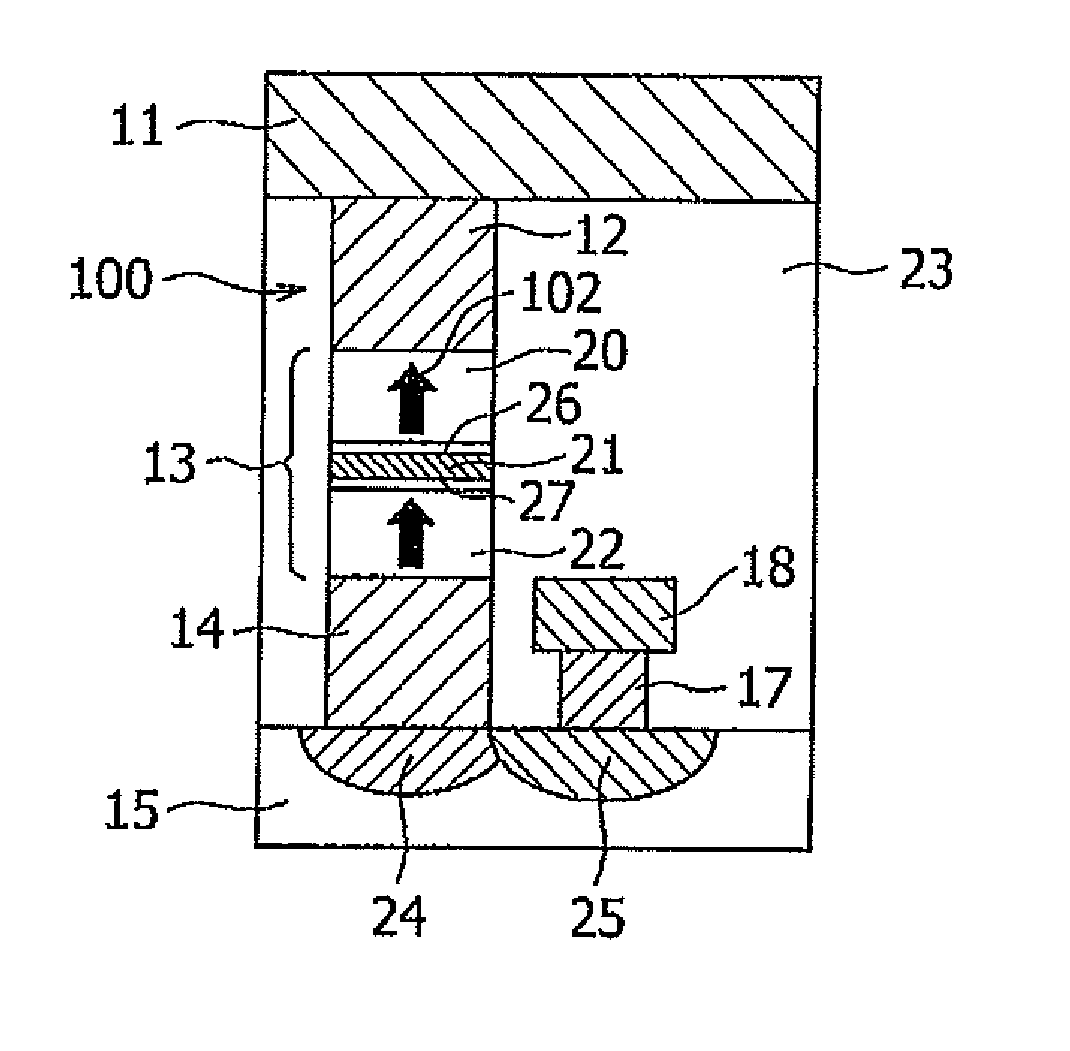
[0057]FIG. 1 is an enlarged cross-sectional view showing a portion of the magnetic memory element 100 of a storage device 10 comprising the magnetic memory element. The magnetic memory element 100 has a magnetic tunnel junction (MTJ) portion 13; this MTJ portion 13 is sandwiched between a lower electrode 14 and an upper electrode 12. The MTJ portion 13 has a structure in which are stacked, in order from the side of the lower electrode 14, a pinned layer 22 (first magnetic layer), first spin polarization enhancement layer 27 (third magnetic layer), insulating layer 21, second spin polarization enhancement layer 26 (fourth magnetic layer), and recording layer 20 (second magn...

second embodiment

[0079]A second embodiment of the invention is explained. The second embodiment is an embodiment in which, in the first embodiment, TbCo is used in the pinned layer. TbCo has oxidation resistance superior to that of TbFeCo, and if the magnetic memory element of this embodiment is used in a storage device, the lifetime of the storage device can be lengthened. Further, the magnetization of TbCo is lower than that of TbFeCo, so that the shape anisotropy energy is reduced, and an increase in the perpendicular-direction magnetic anisotropy energy Ku can be expected. An increase in the perpendicular magnetic anisotropy energy Ku leads to improved thermal stability. When thermal stability of the pinned layer is low, the magnetization direction is disordered upon excessive heating of the magnetic memory element, and the magnetic memory element no longer operates normally. Hence by improving thermal stability using TbCo in the pinned layer, the reliability of the storage device can be improve...

third embodiment

[0081]A third embodiment of the invention is explained. The third embodiment is an embodiment in which TbCo is used as the recording layer in the first embodiment or the second embodiment. TbCo has a magnetic anisotropy energy an order of magnitude greater than that of GdCo, and so by using TbCo in the recording layer, stored data retention characteristics can be improved. In the prior art, if the magnetic anisotropy energy of the recording layer is increased, there is the problem that the write current increases; but in this embodiment the temperature of the recording layer during writing approaches the magnetic compensation temperature, and the magnetization becomes extremely low, so that increases in the write current are suppressed and this problem is alleviated.

[0082]As the TbCo of the recording layer in this embodiment, it is preferable that the Tb composition ratio be in the range 22 to 26 at. %. Similarly to the case of the first embodiment, this is because the magnetic comp...


PUM


Abstract

A magnetic memory element having a memory cell of size 4F2 is provided that realizes a crosspoint-type memory. In the magnetic memory element, a first magnetic layer, a third magnetic layer (spin polarization enhancement layer), an intermediate layer, a fourth magnetic layer (spin polarization enhancement layer), and a second magnetic layer are stacked in order. The intermediate layer is made of an insulating material or a nonmagnetic material. The second magnetic layer is composed of a ternary alloy of gadolinium, iron and cobalt, a binary alloy of gadolinium and cobalt, or a binary alloy of terbium and cobalt. Alternatively, the first magnetic layer is composed of a ternary alloy of terbium, iron and cobalt, or a binary alloy of terbium and cobalt.

Description

[0001]This application is a continuation of co-pending International Application No. PCT / JP2009 / 067237, with an international filing date of Oct. 2, 2009, now abandoned, the subject matter of which is incorporated herein by reference, and claims the foreign priority benefit under 35 USC 119 of Japanese application Serial No. 2008-325640, filed on Dec. 22, 2008, the subject matter of which is incorporated herein by reference.BACKGROUND OF THE INVENTION[0002]1. Field of the Invention[0003]The present invention relates to a magnetoresistance element to read out data using an magnetoresistance effect, and to a storage device using such a magnetoresistance element.[0004]2. Background of the Related Art[0005]In recent years, there have been remarkable increases in the storage capacity of nonvolatile semiconductor storage devices, of which flash memory is representative, and the release of products with capacities of approximately 32 gigabytes have been announced. Nonvolatile semiconductor...

Claims


Application Information

Patent Timeline
IPC IPC(8): G11C11/00H01L29/82
CPCB82Y25/00G11C11/16H01F10/126H01F10/325H01F10/3286H01L43/08H01L43/10H01L43/12H01L27/224H01F10/3254G11C11/1659G11C11/161H10B61/10H10N50/85H10N50/01H10N50/10H01F10/16H10B99/00
Inventor YAMADA, MICHIYAOGIMOTO, YASUSHI
Owner III HLDG 3
Why Eureka
Try Eureka