

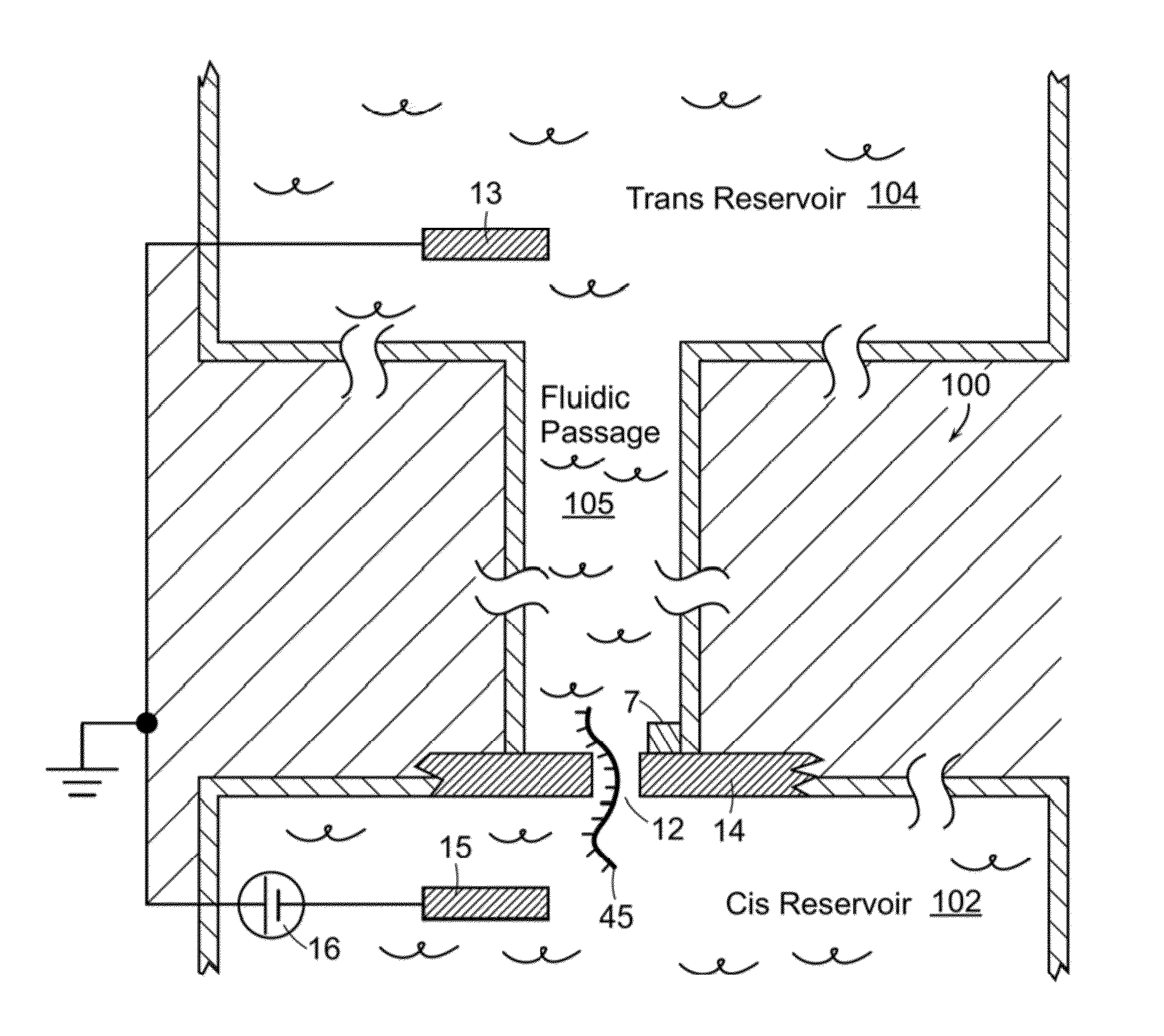
Nanopore Sensor Including Fluidic Passage
a fluid passage and nanopore technology, applied in the field of sensing systems, can solve the problems of limiting the integration density of nanopore devices, affecting the sensitivity of the amphiphilic membrane in which they are provided, and affecting the sensitivity of the amphiphilic membrane in general, so as to achieve high sensitivity, high bandwidth, and large signal
- Summary
- Abstract
- Description
- Claims
- Application Information
AI Technical Summary
Benefits of technology
Problems solved by technology
Method used
Image

Examples
example i
Fabrication of a SiNW FET in a Nanopore Sensor
[0160]SiNWs were synthesized using an Au-nanoparticle-catalyzed chemical vapor deposition (CVD) method. 30 nm-diameter gold nanoparticles (Ted Pella Inc., Redding, Calif.) were dispersed on a silicon wafer coated with a 600 nm-thick layer of silicon oxide (NOVA Electronic Materials Inc., Flower Mound, Tex.). Boron-doped p-type SiNWs were synthesized at 435° C. and 30 torr, with 2.4 standard cubic centimeters per minute (sccm) silane as a silicon source, 3 sccm diborane (100 ppm in helium) as a boron dopant source and 10 sccm argon as the carrier gas. The nominal doping ratio was 4000:1 (Si:B) and the growth time was 20 minutes. The resulting SiNWs were dissolved in ethanol by gentle sonication for ˜10 seconds. Then the NW solution was deposited onto a 50 nm-thick, 100 μm×100 μm silicon nitride TEM membrane grid (SPI supplies. West Chester, Pa.). Electron beam lithography and evaporation of a 60 nm-thick layer of nickel were carried out t...
example ii
Sensitivity Profiling of a SiNW FET In a Nanopore Sensor
[0162]The sensitivity of the SiNW FET sensor of the nanopore sensor was characterized by scanning gate microscopy (SGM). A SiNW FET device was fabricated in accordance with the method of Example I, here with ˜2 μm long channel length to accommodate the limited spatial resolution of SGM. SGM was performed in a Nanoscope IIIa Multi-Mode AFM (Digital Instruments Inc., Tonawanda, N.Y.) by recording the conductance of the nanowire as a function of the position of a −10 V biased conductive AFM tip (PPP-NCHPt, Nanosensors Inc., Neuchatel, SW). The AFM tip was 20 nm above the surface during SGM recording.
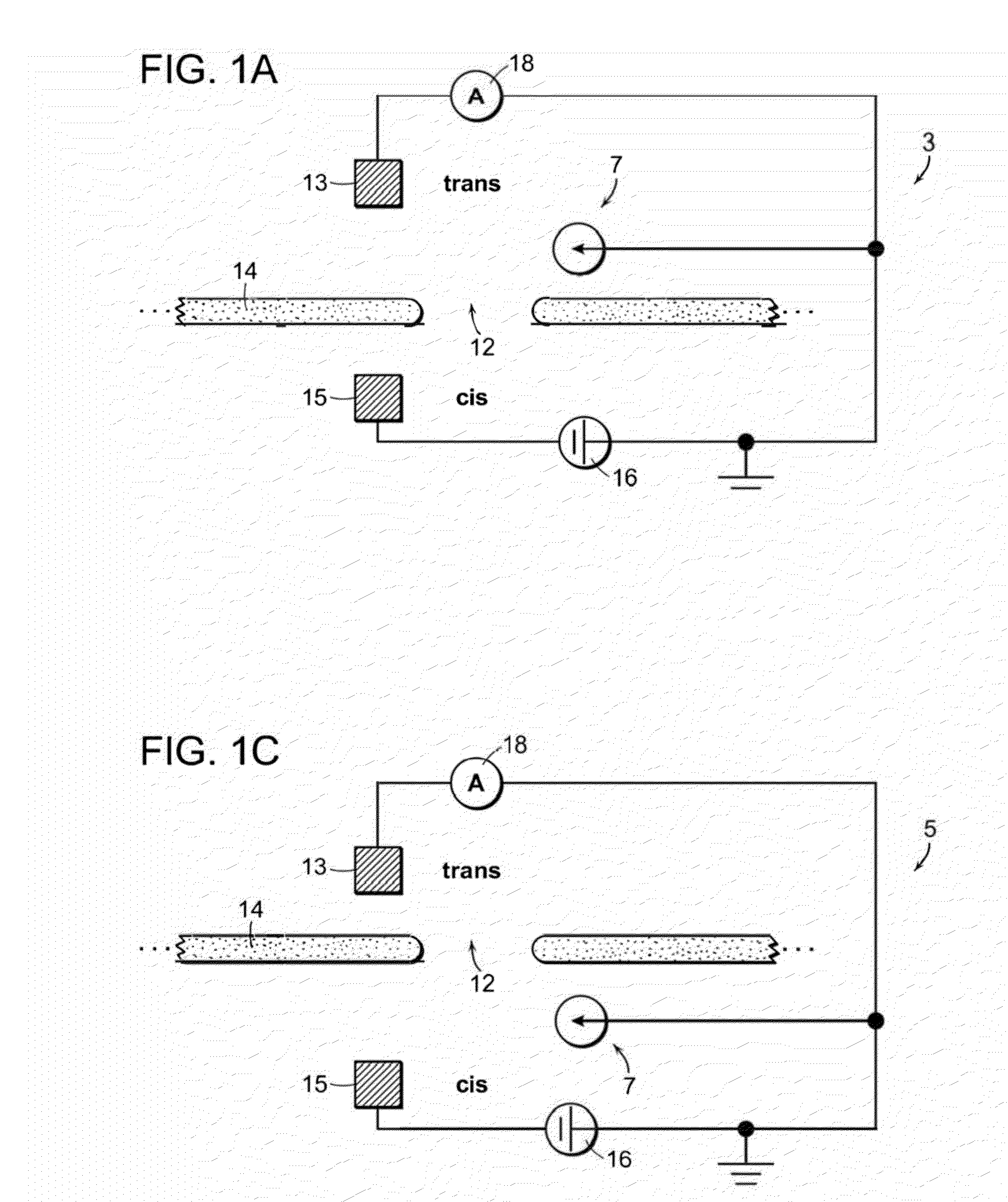
[0163]Prior to formation of a nanopore at the nanowire site, an SGM profile was produced across the nanowire. Then a nanopore was formed at the edge of the nanowire in the arrangement depicted in FIG. 22B. With the nanopore present, the SGM profile of the nanowire was again produced. The SGM profile was determined by averaging the cond...
example iii
Cleaning and Assembly of a Nanowire-Nanopore in a Nanopore Sensor
[0164]The nanowire-nanopore assembly produced by the method of Example I above was cleaned by UV-ozone stripper (Same° International Inc.) at 150° C. for 25 minutes on each side after formation of the nanopore. This cleaning process is preferred to remove any possible carbon deposition on the structure. Then the structure was annealed in forming gas at 250° C.-350° C. for 30 seconds to recover the conductance of the nanowire. A further 25 minute room temperature UV-ozone cleaning was performed on each side of the structure to ensure hydrophilicity of the nanopore just before assembly.
[0165]To assemble the nanowire-nanopore structure with fluidic reservoirs for species translocation through the nanopore, PDMS chambers were sonicated first in DI water, then 70% ethanol and finally pure ethanol, each for ˜30 minutes and then stored in pure ethanol. Just before assembly, PDMS chambers were baked in a clean glass petri dish...
PUM
| Property | Measurement | Unit |
|---|---|---|
| diameters | aaaaa | aaaaa |
| length | aaaaa | aaaaa |
| electrical potential | aaaaa | aaaaa |
Abstract
Description
Claims
Application Information