Low Noise Ultrathin Freestanding Membranes Composed of Atomically-Thin 2D Materials

Active Publication Date: 2018-02-08
NORTHEASTERN UNIV
View PDF4 Cites 15 Cited by
  • Summary
  • Abstract
  • Description
  • Claims
  • Application Information

AI Technical Summary

Benefits of technology

[0012]According to the present invention, in situ fabrication of freestanding membranes onto a perforated substrate does not require transferring sheets of 2D material after its synthesis. As a consequence, the formed membrane retains its pristine quality with no contamination, resulting in ideal substrate

Problems solved by technology
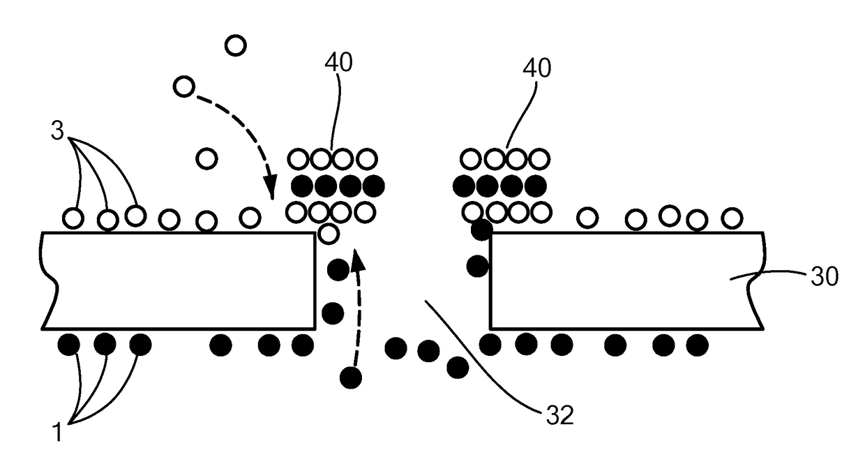
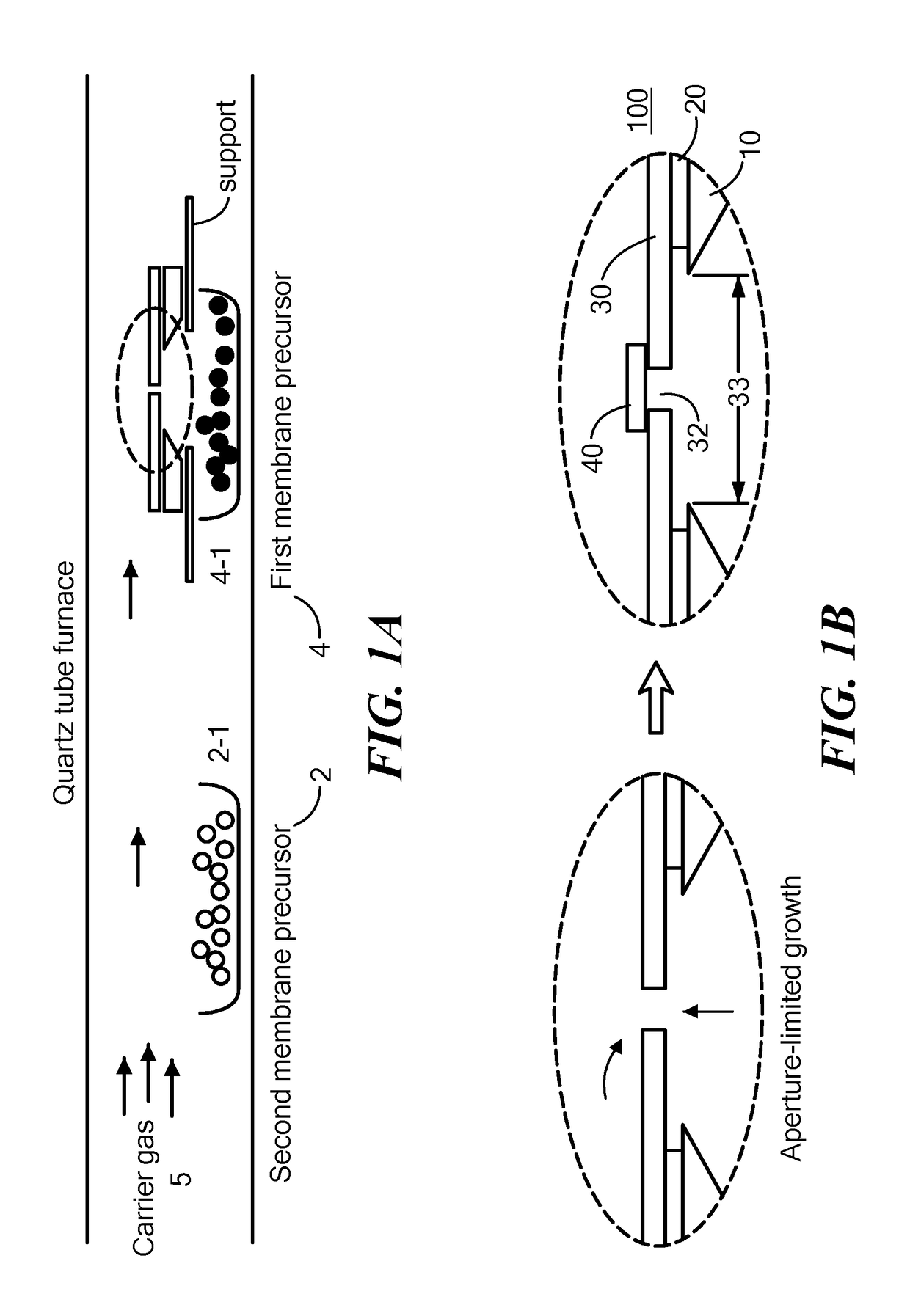
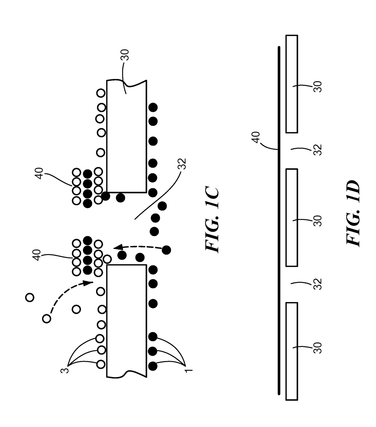
Even though graphene is a good electrical and thermal conductor, its zero band gap property hinders the possibilities in a wide range of potential applications in next generation nanoelectronics and optoelectronics.
[3] Moreover, engineering a band gap of graphene makes the fabrication more complicated and reduces the electronic mobility.
Several groups have recently shown high-resolution DNA detection using mono- and few-layer graphene nanopores [38-41], yet the large noise compared to traditional dielectric material based nanopores and the zero band gap property of graphene hinder the development of graphene-based nanopore sensors to achieve base-resolution detection.
Even though a finite band gap can be engineered in pristine graphene, this increases the fabrication complexity and reduces the electronic mobility.
Another issue with graphene nanopores is that DNA sticks a lot to the pore wall as well as the surface during the translocation process due the strong π-π interaction between graphene and DNA, which could prove very challenging for nucleobase detect

Method used


Image

  • Low Noise Ultrathin Freestanding Membranes Composed of Atomically-Thin 2D Materials
  • Low Noise Ultrathin Freestanding Membranes Composed of Atomically-Thin 2D Materials
  • Low Noise Ultrathin Freestanding Membranes Composed of Atomically-Thin 2D Materials

Examples


example 1

Fabrication of Freestanding Ultrathin MoS2 Membranes

[0104]Substrates for nanopore fabrication were 5 mm×5 mm square Si chips with a 100-nm-thick SiN film deposited on a 2.5 μm thick thermal SiO2 layer. The oxide layer helps to reduce electrical noise. The SiN film was protected with a 950 PMMA etch mask, and a small (2 μm×2 μm) region with a pattern of four 600 nm-diameter holes and a central 1.5 μm diameter hole was exposed using Nabity NPGS e-beam writing software on a Hitachi S-4800 scanning electron microscope. Exposed PMMA was developed with 3:1 isopropyl alcohol and methyl isobutylketone. The SiN film was etched to AFM- and ellipsometry-calibrated thickness in a Technics Micro-RIE Series 800 etcher using sulfur hexafluoride (SF6) at 300 mTorr and 150 W. PMMA was removed using acetone, and chips were cleaned with hot piranha solution followed by warm water to remove residual PMMA.

[0105]MoS2 membranes were synthesized using an atmospheric-pressure CVD process in a split tube fur...

example 2

Structural Characterization of MoS2 Membranes.

[0107]FIG. 2A shows bright-field (BF) TEM images of freestanding MoS2 membranes synthesized, without a substrate, onto micron-scale holes prefabricated in a thin sheet of SiN. Panels (i)-(iv) of FIG. 2A show high magnification TEM images of four different MoS2 membrane devices. Some holes are partially covered with multiple layers of MoS2, which possibly could be due to the insufficient nucleation time during CVD. It is noteworthy that unintentional wrinkles could be seen in some MoS2 membranes grown across holes, which may be due to stress exerted on the membranes as they freely suspend over the free aperture (see, e.g., FIG. 2A(iii)). Different domains of monolayer and multilayer MoS2 were observed in membranes grown across submicron aperture regions.

[0108]FIG. 2B shows high resolution TEM (HRTEM) images of the MoS2 membrane analyzed in the highlighted region as depicted in FIG. 2A(i) with a dashed box. In FIG. 2B it is clear that ther...

example 3

Electrical Characterization of MoS2 Membranes Containing Nanopores

[0112]Following optimization of hole-free membrane growth, complete MoS2 membranes were grown on several devices, and a TEM beam was used to fabricate nanopores in these membranes in order to study ion transport through the pores.

[0113]Because of the extremely thin membrane structure, only brief (about 1-2 sec) exposure times using a focused beam were sufficient to produce nanopores; great care was taken to avoid large pore formation, e.g., by reduction of spot size and beam current.

[0114]Following the fabrication of several pores of different diameters, the chips were assembled into a custom-made PTFE cell as shown in FIG. 6A. Prior to obtaining measurements, a chip was glued onto the top PTFE portion of the cell using a quick-curing elastomer, and a second layer of glue was applied to the membrane such that only about 1 mm2 was exposed, in order to minimize capacitance-mediated noise. After elastomer curing, the cel...


PUM

PropertyMeasurementUnit
Temperatureaaaaaaaaaa
Timeaaaaaaaaaa

Abstract

The invention provides methods for direct growth of low noise, atomically thin freestanding membranes of two-dimensional monocrystalline or polycrystalline materials, such as transition metal chalcogenides including molybdenum disulfide. The freestanding membranes are directly grown over an aperture by reacting two precursors in a chemical vapor deposition process carried out at atmospheric pressure. Membrane growth is preferentially over apertures in a thin sheet of solid state material. The resulting membranes are one or a few atomic layers thick and essentially free of defects. The membranes are useful for sequencing of biopolymers through nanopores.

Description

[0001]This application claims the priority of U.S. Provisional Application Nos. 62 / 118,795 filed 20 Feb. 2015 and entitled “Aperture-Limited Fabrication of Freestanding MoS2 Membranes” and 62,119,675 filed 23 Feb. 2015 and entitled “Aperture-Limited Fabrication of Freestanding MoS2 Membranes”. Both provisional applications are hereby incorporated by reference in their entirety.BACKGROUND[0002]The ability to exfoliate single- and few-layer graphene flakes from bulk graphite opened up new avenues into the physics of two-dimensional materials. [1,2][0003]Even though graphene is a good electrical and thermal conductor, its zero band gap property hinders the possibilities in a wide range of potential applications in next generation nanoelectronics and optoelectronics. [3] Moreover, engineering a band gap of graphene makes the fabrication more complicated and reduces the electronic mobility. [4,5] In this regard, molybdenum disulfide (MoS2), a layered transition metal dichalcogenide (TMDC...

Claims


Application Information

Patent Timeline
IPC IPC(8): C25B9/10C12Q1/68C01B32/186G01N33/487G01N27/447C25B9/23
CPCC25B9/10G01N33/48721G01N27/4473C01B32/186C12Q1/6869G01N27/44791C25B9/23
Inventor WADUGE, PRADEEPKAR, SWASTIKWANUNU, MENILARKIN, JOSEPHBILGIN, ISMAIL
Owner NORTHEASTERN UNIV
Why Eureka
Try Eureka