Multilayer ceramic capacitor

a multi-layer ceramic and capacitor technology, applied in the direction of fixed capacitors, stacked capacitors, fixed capacitor details, etc., can solve the problems of reliability degradation and insulation resistance reduction between internal electrodes, and achieve the effect of improving the capacitance of multi-layer ceramic capacitors, reducing or preventing the formation of mg—ni protrusions

Active Publication Date: 2022-03-31
MURATA MFG CO LTD
View PDF7 Cites 3 Cited by
  • Summary
  • Abstract
  • Description
  • Claims
  • Application Information

AI Technical Summary

Benefits of technology

[0042]The Ni-containing grains are not particularly limited in terms of distribution of the Ni concentration as long as the grains include the low-Ni-concentration region and the high-Ni-concentration region. However, core-shell grains are preferable. In the core-shell grains, the high-Ni-concentration region occupies a core portion while the low-Ni-concentration region occupies a shell layer. In this case, there may be a single core portion in the grains, or there may be two or more. The entire core portion may be covered with the shell layer. Alternatively, the core portion may be partially exposed at the grain surface. Preferably, the Ni-containing grains include the high-Ni-concentration region in an area ratio of about 9% or more, for example. This makes it possible to achieve the advantageous effects of improving the insulating properties and high temperature reliability.
[0043]Preferably, for example, the content of the rare earth element (Re) with respect to 100 mol parts of titanium (Ti) in the high-Ni-concentration region is about 1.3 times or more than the content of the rare earth element (Re) with respect to 100 mol parts of titanium (Ti) in the low-Ni-concentration region. To make the Re concentration in the high-Ni-concentration region high in this manner enables the advantageous effects of improving the high temperature reliability to be obtained.
[0044]The distributions of Ni concentration and Re concentration in the grains can be measured by making an analysis at a cross section of the dielectric layers with TEM-EDX, and further by making an image analysis of the obtained cross-sectional EDX image. For example, the Ni concentration on the cross-sectional EDX image is quantified and mapped to classify the low-Ni-concentration region and the high-Ni-concentration region in the main crystal grains based on the obtained mapping image. The main crystal grains including both the low concentration region and the high concentration region are regarded as Ni-containing grains, and the number ratio thereof is obtained. The areas of the low-Ni-concentration region and the high-Ni-concentration region on the cross-sectional EDX image can be obtained, and the area ratio of the high-Ni-concentration region can be obtained therefrom.
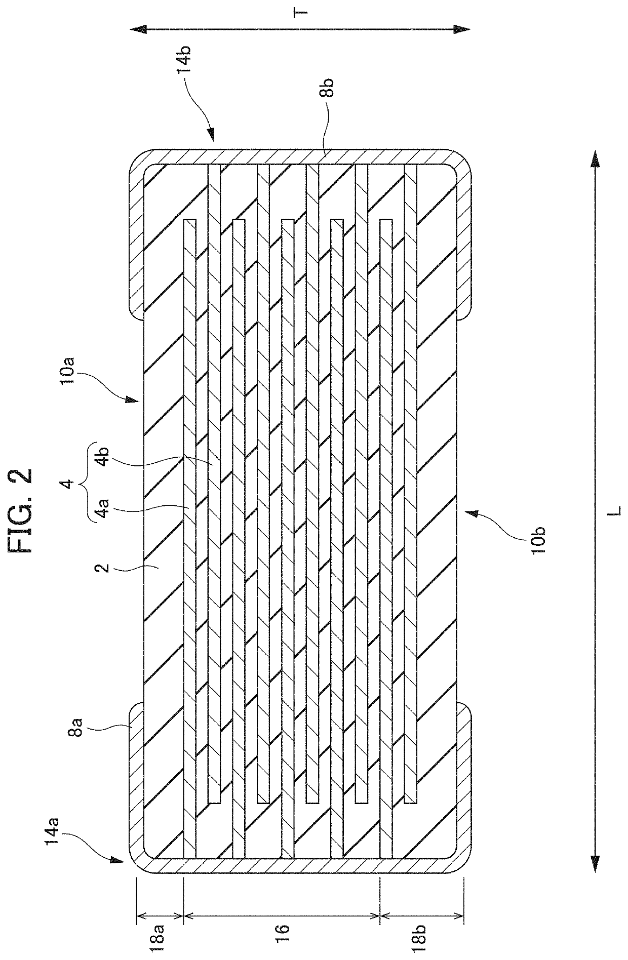
[0045]The thickness of each of the dielectric layers in the inner layer is preferably about 1.0 μm or less, and particularly preferably about 0.4 μm or less, for example. Thinning the dielectric layers makes it possible to improve the capacitance of the multilayer ceramic capacitor. In the multilayer ceramic capacitor of the present preferred embodiment, it is possible to reduce or prevent the formation of the Mg—Ni protrusions at the interface between the dielectric layers and the internal electrode layers. Therefore, thinning does not deteriorate the insulating properties (IR, short-circuit ratio), and reliability can be improved. However, an excessively-thinned dielectric layers make it difficult to reduce or prevent the deterioration of the insulating properties. The thickness of the dielectric layers is typically about 0.15 μm or more, for example.
[0046]The thickness of the dielectric layers in each of the first outer layer and the second outer layer is preferably about 9.5 μm or more and about 30 μm or less, and more preferably about 9.5 μm or more and about 20 μm or less, for example. The dielectric layers in the first outer layer and the second outer layer may be a single layer, or may be a multilayer body including a plurality of layers. The dielectric layers in the first outer layer and the dielectric layers in the second outer layer may be the same or may be different in thickness.
[0047]The compositions of the dielectric layers in each of the inner layer, the first outer layer, and the second outer layer are not limited as long as they satisfy the requirements described above. For example, the compositions of the dielectric layers in the inner layer may be same as or different from the composition of the dielectric layers in the first outer layer and the second outer layer. The compositions of the dielectric layers in the first outer layer and the second outer layer may be same as or may be different from each other. It is preferable that the total number of layers of the dielectric layers in the inner layer, the first outer layer, and the second outer layer are fifteen or more and seven hundred or less, for example.Internal Electrode Layer

Problems solved by technology

However, reducing the thickness of the dielectric layers may lead to a reduction in the insulation resistance between the internal electrode layers, which results in a problematic degradation of reliability.

Method used


Image

  • Multilayer ceramic capacitor
  • Multilayer ceramic capacitor
  • Multilayer ceramic capacitor

Examples


examples 1 to 67

[0065]In Examples 1 to 67, the compositions of the dielectric layers were varied to manufacture multilayer ceramic capacitors, which were evaluated thereafter. The compositions of the dielectric layers and the characteristics of the capacitor are summarized in Table 1.

[0066]A BamTiO3 powder was prepared as a main component raw material. Here, m refers to the A / B molar ratio, i.e., Ba / Ti molar ratio, of the perovskite compound (ABO3). The BamTiO3 powder used had a particle size D50 of about 140 nm and a c-axis / a-axis ratio of the perovskite structure of about 1.0090. Next, the prepared BamTiO3 powder was weighed and wet-mixed by a ball mill to break up aggregates.

[0067]Besides the main component raw material, the additive component raw materials (Ni, Re, Mg, Mn, Si, Al, V) were weighed. As the additive component raw materials, nickel oxide (NiO), rare earth oxides (Dy2O3, etc.), magnesium carbonate (MgCO3), manganese carbonate (MnCO3), silicon oxide (SiO2), aluminum oxide (Al2O3), an...

examples 68 to 81

[0074]The amounts of the raw materials were adjusted to provide compositions of the dielectric layers and the side margin portions in the manufactured multilayer ceramic capacitors, as shown in Table 3. Except for the above, multilayer ceramic capacitors were manufactured in the same or substantially the same manner as in Example 6.

example 82

[0075]In the manufactured multilayer ceramic capacitor, the amounts of the raw materials were adjusted to provide compositions of the dielectric layers and the side margin portions, as shown in Table 3. Except for the above, a multilayer ceramic capacitor was manufactured in the same or substantially the same manner as in Example 1.

(2) Evaluation

[0076]The manufactured multilayer ceramic capacitors were evaluated for various characteristics as follows.

Composition Analysis

[0077]On the cross section of the multilayer ceramic capacitors, the side margin portion was analyzed by laser ablation ICP-MS. Furthermore, portions other than the inner region (22) were removed by ablating, and after being pulverized, the internal electrode Ni was removed by a magnet. The remaining ceramics were analyzed by ICP-MS to analyze the compositions of the dielectric layers.

Ni and Re Distributions in Grains

[0078]The cross sections of the multilayer ceramic capacitors were subjected to mapping analysis usin...


PUM

PropertyMeasurementUnit
thicknessaaaaaaaaaa
thicknessaaaaaaaaaa
thicknessaaaaaaaaaa

Abstract

A multilayer ceramic capacitor includes a base body including first and second main surfaces, first and second side surfaces, first and second end surfaces, and dielectric layers and internal electrode layers, and external electrodes at the first and second end surfaces, and electrically connected to the internal electrode layers. The base body includes an inner layer, first and second outer layers, first and second side margin portions. The dielectric layers in the inner layer and the first and second outer layers include main crystal grains including barium and titanium, and with respect to 100 parts by mol of titanium, nickel in an amount of about 0.2 to about 3.0 parts by mol, and at least one rare earth element selected from yttrium, praseodymium, neodymium, samarium, europium, gadolinium, terbium, dysprosium, holmium, erbium, thulium, ytterbium, and lutetium in an amount of about 0.6 parts to about 2.0 parts by mol.

Description

CROSS REFERENCE TO RELATED APPLICATIONS[0001]This application is based on and claims the benefit of priority from Japanese Patent Application No. 2020-165987, filed on Sep. 30, 2020, the contents of which are incorporated herein by reference.BACKGROUND OF THE INVENTION1. Field of the Invention[0002]The present invention relates to a multilayer ceramic capacitor.2. Description of the Related Art[0003]With the miniaturization of electronic devices, such as mobile phones, and high speed CPUs, the demand for multilayer ceramic capacitors (MLCC) has been increasing. A multilayer ceramic capacitor, which includes dielectric layers and internal electrode layers stacked alternately in the structure, is small, yet exhibits a large capacitance due to thin dielectric layers exhibiting high permittivity. Multilayer ceramic capacitors containing various materials are known, and those containing barium titanate (BaTiO3)-based compounds in dielectric layers and a base metal such as nickel (Ni) in ...

Claims


Application Information

Patent Timeline
Patent Type & Authority Applications(United States)
IPC IPC(8): H01G4/30H01G4/012H01G4/12H01G4/008
CPCH01G4/30H01G4/008H01G4/1227H01G4/012H01G4/232
Inventor ISOTA, SHINYASASABAYASHI, TAKEHISAUCHIDA, KAZUHISAHASHIMOTO, HIDEYUKIOSHIMA, YUTA
Owner MURATA MFG CO LTD
Why Eureka
Try Eureka