

Cleaning compositions for removing etching residue and method of using
a technology of cleaning composition and etching residue, which is applied in the direction of detergent compounding agents, washing machines, instruments, etc., can solve the problems of substantially impossible removal of resist mask, ineffective removal of sidewall organometallic polymer, and above-mentioned solvents, so as to increase the stability and effectiveness of cleaning compositions
- Summary
- Abstract
- Description
- Claims
- Application Information
AI Technical Summary
Benefits of technology
Problems solved by technology
Method used
Image

Examples
example 1
Example 1 illustrates the removal of a photoresist from a substrate using different stripping compositions of the present invention. The substrate is treated in a conventional manner prior to the treatment of the substrate with the stripping compositions of the present invention.
More specifically, wafer substrates were spun in a commercially available spinning apparatus with the photoresist K.T.I. 820 at spinning speeds ranging from 1000 to 5000 RPM resulting in the formation of films having a thickness of about 0.5-2.5 microns on the substrate. After thus coating the substrate, the substrate was heated for about 10-20 minutes at 80.degree. C.-90.degree. C. to drive out any traces of solvent from the photoresist. Next, the photoresist was selectively exposed using an image pattern transfer technique as known in the art. The exposed areas of the positive photoresist were solubilized in a developer solution. After such development, the pattern on the wafer was cleaned using a spray ri...
example 2
Example 2 illustrates the removal of a polyimide resist coating from a substrate using stripping compositions of the present invention. As in Example 1, a conventional coating method was utilized.
More specifically, wafer substrates were coated with ASAHI G-6246-S negative imageable polyimide to a thickness of 16 microns. The coated wafers were baked at 250.degree. C. to remove the solvent present in the polyimide. The polyimide coating was then exposed in a Nikon Stepper with a 350 mJ dose and developed in the Asahi A-145 / C-210 developer. The wafers were then immersed in a bath containing a stripping composition and processed in the stripping bath as described in Example 1 according to the temperatures and times as set forth in Table III below.
example 3
Example 3 illustrates the removal of a polyimide coating from a substrate having multiple layers of materials thereon.
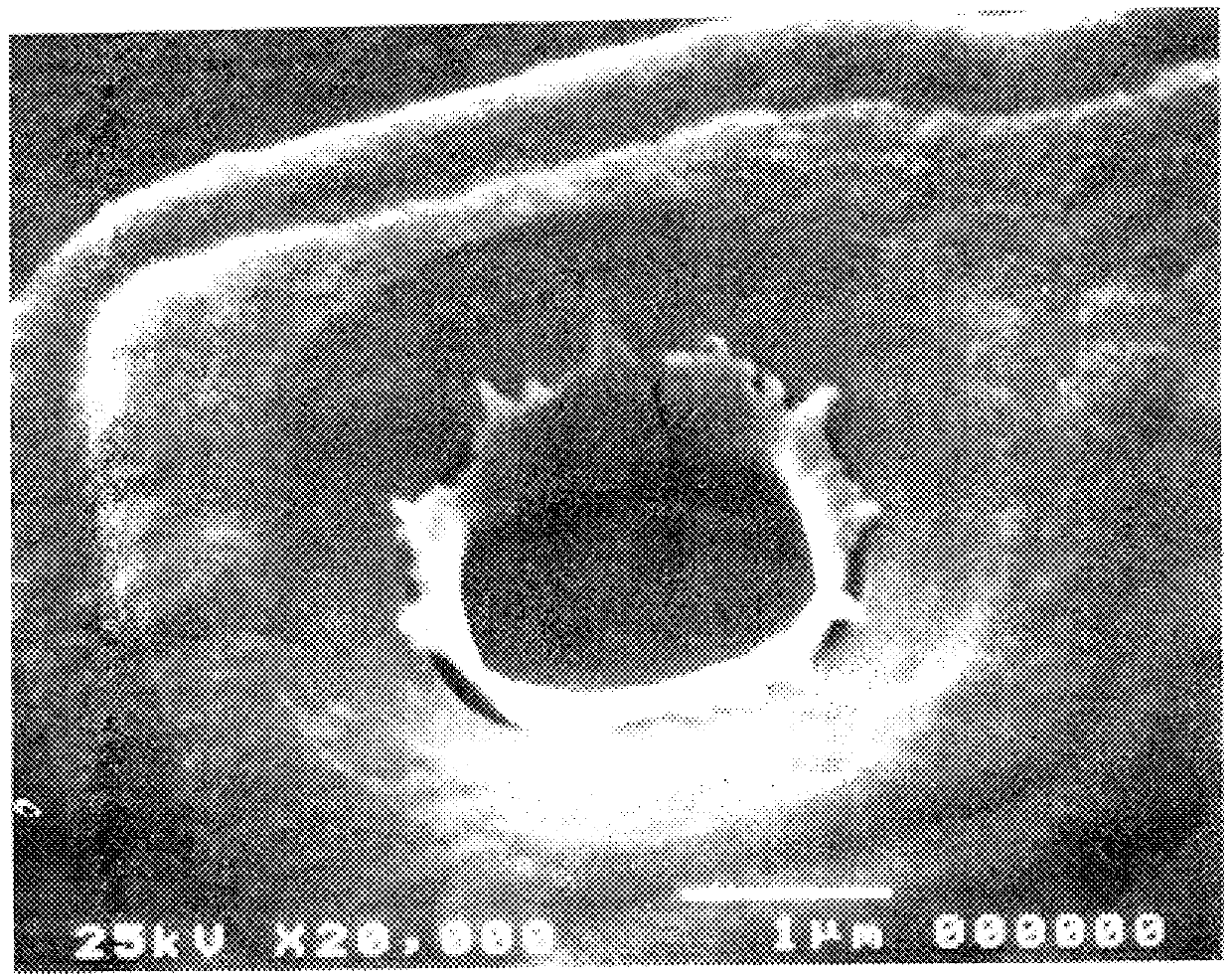
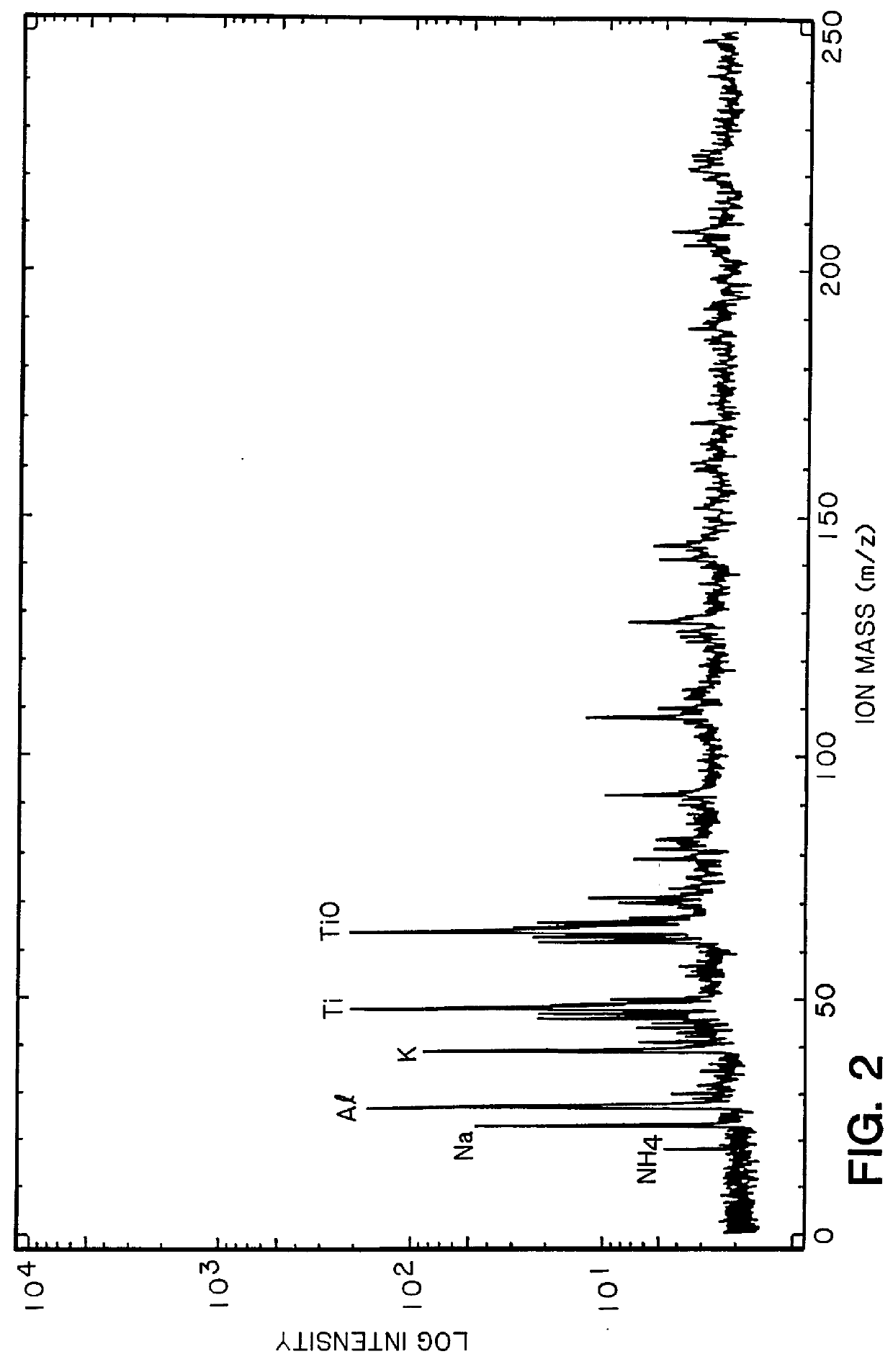
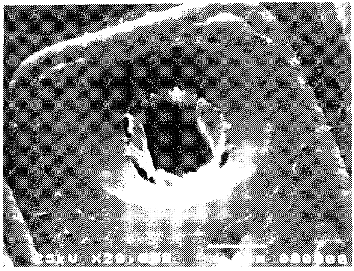
A coating of Ciba Geigy Proimide 293 was spun onto a 3" Gallium / Arsenide wafer to a thickness of 4 microns. The polyimide coating was fully cured at 400.degree. C. for 30 minutes. Silicon oxide was then deposited to a thickness of 1000 Angstrom on the polyimide coated surface. Thereafter, a positive photoresist was applied over the silox surface and a pattern created in the photoresist through the steps of exposure and resist development. The image created was then transferred from the photoresist to the silox surface by etching the silicon oxide using a plasma etching technique as known in the art. The pattern was further transferred to the polyimide layer by etching the photoresist and polyimide simultaneously. This procedure resulted in a pattern which covered all the regions on which no metal film was desired. Thereafter, a titanium / tungsten metal film was deposi...
PUM
| Property | Measurement | Unit |
|---|---|---|
| temperature | aaaaa | aaaaa |
| temperature | aaaaa | aaaaa |
| temperature | aaaaa | aaaaa |
Abstract
Description
Claims
Application Information