

Imaged article on polymeric substrate
a polymeric substrate and image technology, applied in thermography, conductive material removal by irradiation, instruments, etc., can solve the problems of sudden increase in surface temperature for a short time, each method has limitations, and the method is undesirable, so as to prevent premature tearing of the coating during testing and increase the thickness
- Summary
- Abstract
- Description
- Claims
- Application Information
AI Technical Summary
Benefits of technology
Problems solved by technology
Method used
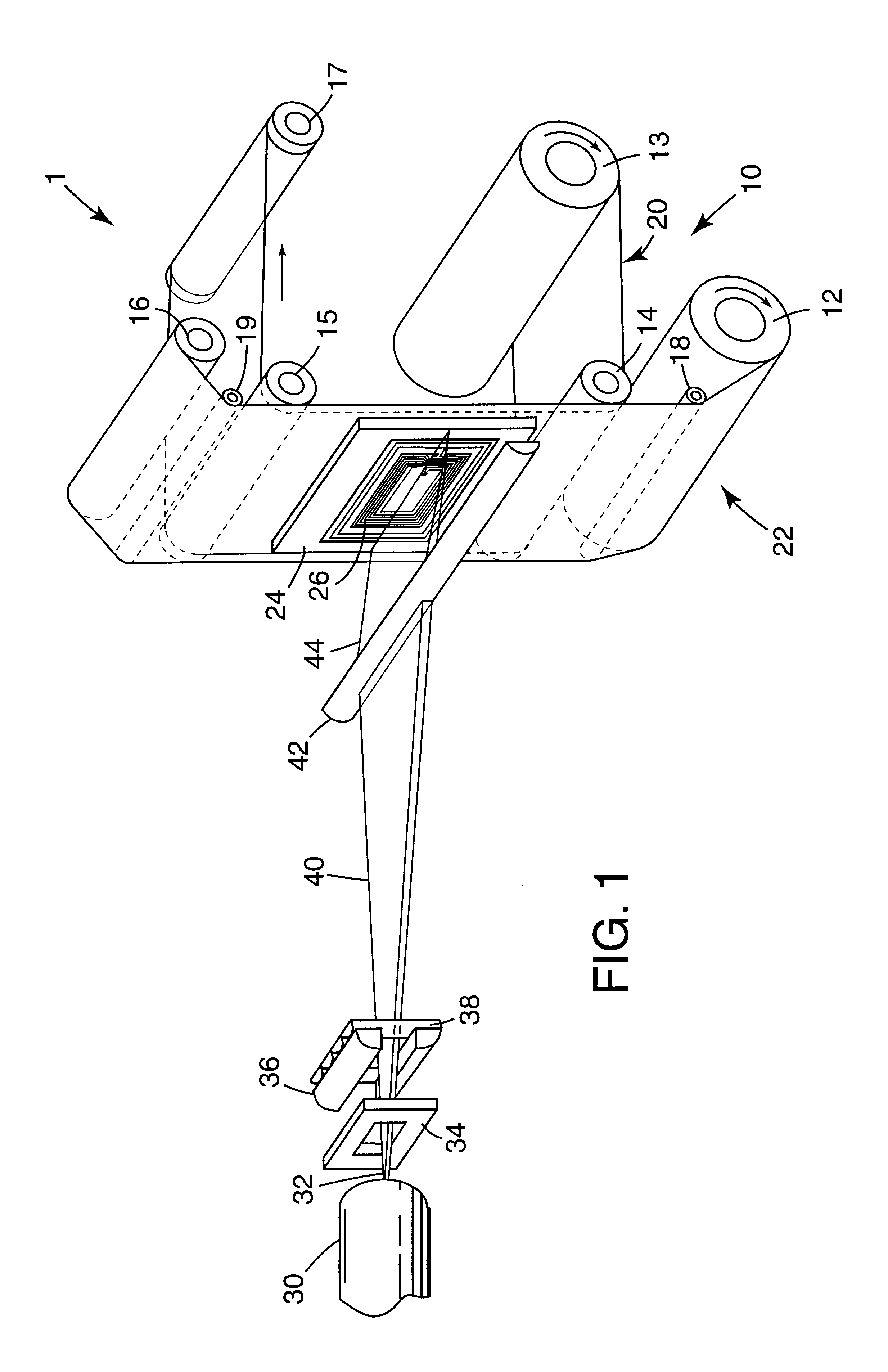
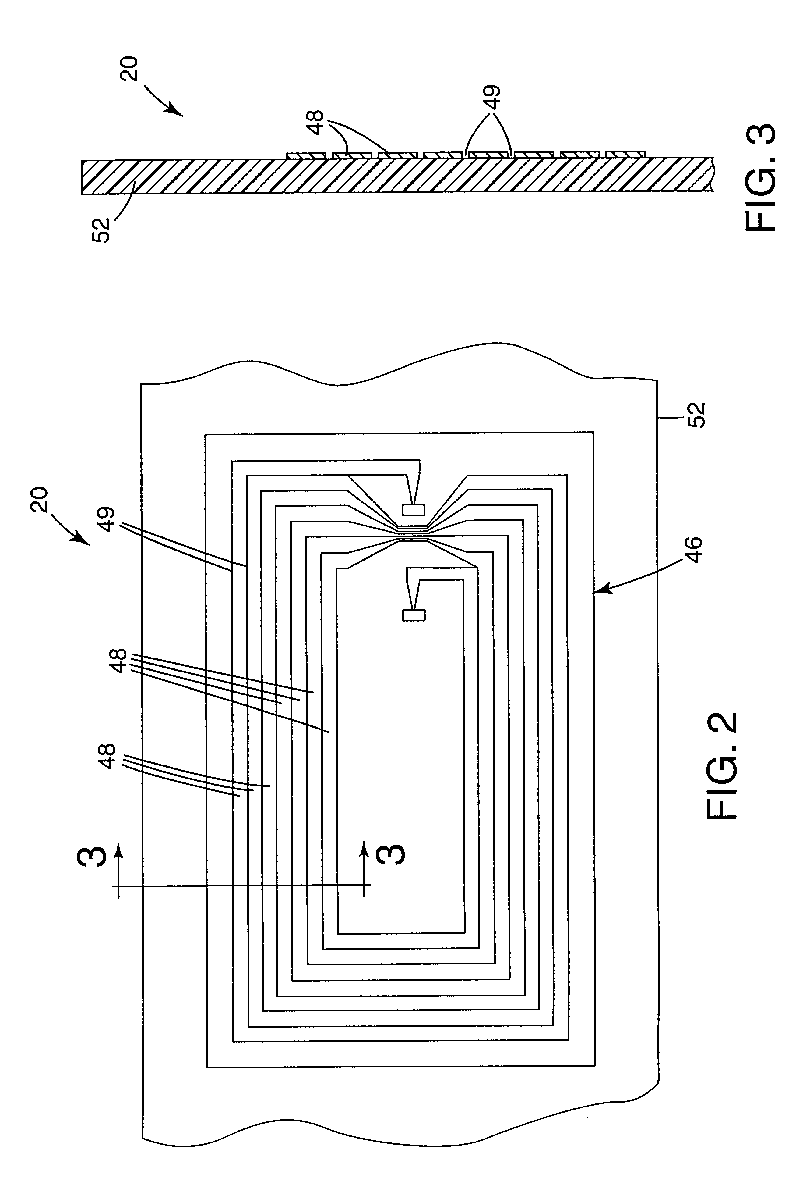
Image

Examples
examples 2 and 3
were made and tested as in Example 1 except the fluence was approximately 200 and 300 mJ / cm.sup.2, respectively. The pattern in the copper coating had good resolution. The fine features were as small as 75 .mu.m wide metal lines and 75 .mu.m wide spaces. Also, there were no electrical shorts between the lines or breaks within the lines.
For comparison, Comparative Examples 1 and 2 were made like Example 1 except for the output energy of the laser. Comparative Example 1 was exposed to a fluence of 150 mJ / cm.sup.2, and Comparative Example 2 was exposed to a fluence of 400 mJ / cm.sup.2 respectively. The exposed metal in Comparative Example 1 was not removed because the fluence used was insufficient to disrupt the interface. In Comparative Example 2, electrical shorts were observed in the patterned copper because the fluence was sufficient to ablate the metal and some of the ablated molten metal re-deposited onto the metal coated surface of the sample.
EXAMPLE 4
This example illustrated the...
example 4
manner similar to Example 1 except a different energy source and optical train were used, some of the conditions were changed, and a different cleaning method was used. The energy source was an infrared laser (Model 2660 Nd:YAG Infrared Laser available from Excel Technology Inc., Hauppauge, N.Y.) operating at a wavelength of 1.06 .mu.m, a repetition rate of 2000 Hz, an energy per pulse of 0.6 mJ, and a pulse width of 200 ns. The laser light incident on the metal coating was a dot or point, in contrast to the line or narrow rectangle of light in example 1 (as shown in FIG. 1). The optical train consisted of only a round piano-convex lens with focal length of 10 cm. There was no beam shaper, homogenizer, or cylindrical lens. No mask and no protective web were used. The resulting fluence reaching the metal surface was determined from the energy output of the laser as measured by a joulemeter (Model J3-09 available from Molectron, Inc. Portland, Oreg.) and the area irradiated on the sur...
example 5
This example illustrated the use of a metal oxide coating on the substrate.
PUM
 Abstract
Description
Claims
Application Information