Method for achieving improved epitaxy quality (surface texture and defect density) on free-standing (aluminum, indium, gallium) nitride ((al,in,ga)n) substrates for opto-electronic and electronic devices

a technology of gallium nitride and surface texture, applied in the field of improving the epitaxy quality of (al, in, ga) n films, can solve the problems of limiting the quality of the epi and device layer, the coefficient of thermal expansion (cte)-matched, and the inability to match lattice-matched gan substrates of suitable quality and size, and the material is non-uniform in morphology and crystalline quality

Inactive Publication Date: 2002-09-10
WOLFSPEED INC
View PDF10 Cites 350 Cited by
  • Summary
  • Abstract
  • Description
  • Claims
  • Application Information

AI Technical Summary

Problems solved by technology

A primary reason for the pervasive character of such research is that free-standing (FS), coefficient of thermal expansion (CTE)--matched, and lattice-matched GaN substrates of suitable quality and size are unavailable.
Without homoepitaxial or native substrates, misfit dislocations will form due to lattice mismatch at the epitaxy-substrate interface, and cracking and bowing will occur due to the CTE mismatch, thereby limiting the quality of the epi and device layers.
Typically, to make higher quality devices, very difficult and complicated overgrowth techniques such as ELOG (epitaxial lateral overgrowth) or LEO (lateral epitaxial overgrowth) or Pendeo-epitaxy are employed, but the resulting material is non-uniform in morphology and crystalline quality.
Further, the resulting material typically has a high carrier concentration due to impurity incorporation from the masking material.
The lack of a suitable quality lattice-matched (Al,In,Ga)N substrate has impeded (Al,In,Ga)N device developers from realizing the full potential of the (Al,In,Ga)N device capabilities and slowed the development of this material system.
The complexity and difficulties attendant the lateral overgrowth techniques have prevented such approach from being satisfactorily commercially used.
High pressure crystal growth has been successful in producing small platelets (<20 mm diameter and <1-2 mm thick) of less than 300 square millimeters area of single crystal GaN but the GaN crystals have several problems.
This technique produces small platelets and the scalability is difficult and the cost of the process is quite large compared to other alternatives.
Further, dopant and conductivity control of the crystal is very difficult due to the technique.
Another disadvantage is that high unintentional impurity levels are present in the crystal including oxygen, which make the substrates conductive.
These high levels of impurities limit the frequency range of devices produced on the substrates due to parasitic capacitances between device layers and charge in the substrate and may inhibit epitaxy nucleation on the substrate at sufficiently high impurity concentrations.
Currently, the boule diameter is limited to 13 millimeters, severely limiting the production of lost cost, high volume devices.
Another issue with these substrates is the extremely high oxygen level, on the order of parts per million (ppm), which will likely reduce the thermal conductivity of the substrates, making them less advantageous for high frequency, high power devices.
In addition to affecting the thermal conductivity, the high impurity incorporation in these substrates inhibits the production of controlled electrical conductivity type substrates, namely p-type substrates.
These substrates are difficult to dope heavily by conventional techniques, making them less advantageous for vertical opto-electronic device structures.
In the case of AlN substrates, the substrate and associated devices are disadvantaged by high ionization or activation energy of acceptors and donors in the crystal, as compared to GaN substrates.
LAO and LGO are closely lattice-matched substrates (compared to SiC and sapphire) and are available in reasonable quality and size, however, several issues exist that prevent their applicability to the GaN material system.
Most importantly, LAO and LGO materials suffer from low decomposition temperatures preventing them from being easily used for GaN growth at typical growth temperatures.
Li and Ga desorption and diffusion from the substrate into the epitaxial film and growth environment make nucleation and high quality, impurity-free growth very difficult, thus limiting the applicability of this substrate.
Limited process conditions are employed to grow on these substrates due to their high susceptibility to decomposition under H.sub.2.
Non-uniform polarity of the substrate surface is also an issue, typically causing mixed polarity domains in the GaN epitaxial film.
The fabrication of vertical devices structures on such substrates also involves issues of doping and suppression of decomposition.
Because there have been no large area, freestanding GaN wafers commercially and readily available, there has been limited opportunity to develop the conditions to produce high quality epitaxial layer growth on FS GaN.
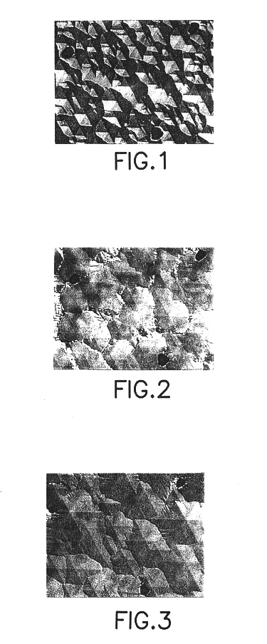
A significant issue relating to growth on FS GaN "as grown" or unfinished surfaces is that appreciable MOVPE (Metal Organic Vapor Phase Epitaxy) thickness has to be deposited to smooth out hillock morphology from the HVPE GaN.
Growing thicker layers of epitaxy on the FS GaN substrate smooths out the "as grown" or unfinished FS GaN morphology, but at the expense of increased cost and longer growth time for a device structure, which in turn increases the cost of the device structure growth and reduces the throughput and profitability of the vapor phase epitaxy (VPE) reactor operation.
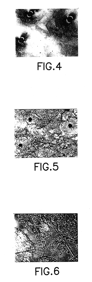
Another issue related to homoepitaxial growth on FS GaN substrates is that the backside of the GaN wafer (N-face) tends to decompose during growth.
This decomposition tends to interrupt the epi growth surface.
Decomposition products escaping from the backside of the wafer are transported to the growth area disturbing the growth conditions and causing interrupted morphology.
The substrate preparation, interface preparation upon heat-up and substrate cleaning, also create issues in MOVPE GaN growth on FS GaN substrates.
General reactor conditions may also affect epitaxial morphology for growth on FS GaN, resulting in poor interrupted morphologies.
Potential impurity and structural damage at the interface leading to charge accumulation at the substrate-epi interface is a potential issue for the use of FS (Al, Ga, In)N in high frequency electronic devices.

Method used


Image

  • Method for achieving improved epitaxy quality (surface texture and defect density) on free-standing (aluminum, indium, gallium) nitride ((al,in,ga)n) substrates for opto-electronic and electronic devices
  • Method for achieving improved epitaxy quality (surface texture and defect density) on free-standing (aluminum, indium, gallium) nitride ((al,in,ga)n) substrates for opto-electronic and electronic devices
  • Method for achieving improved epitaxy quality (surface texture and defect density) on free-standing (aluminum, indium, gallium) nitride ((al,in,ga)n) substrates for opto-electronic and electronic devices

Examples


Embodiment Construction

The disclosures of the following United States Patents and United States Patent Applications are hereby incorporated herein by reference in their respective entireties:

U.S. patent application Ser. No. 08 / 188,469 filed Jan. 27, 1994 in the names of Michael A. Tischler, et al., now issued as U.S. Pat. No. 5,679,152;

U.S. patent application Ser. No. 08 / 955,168 filed Oct. 21, 1997 in the names of Michael A. Tischler, et al.;

U.S. patent application Ser. No. 08 / 984,473 filed Dec. 3, 1997 in the names of Robert P. Vaudo, et al.;

U.S. patent application Ser. No. 09 / 179,049 filed Oct. 26, 1998 in the names of Robert P. Vaudo, et al.;

U.S. patent application Ser. No. 09 / 524,062 filed on Mar. 13, 2000 in the names of Robert P. Vaudo, et al.; and

U.S. patent application Ser. No. 09 / 339,510 filed on Jun. 24, 1999 in the names of Barbara A. Landini, et al. for "SILICON CARBIDE EPITAXIAL LAYERS GROWN ON SUBSTRATES OFFCUT TOWARDS ."

As used herein, the term "free-standing" or "FS" in reference to a subs...


PUM

PropertyMeasurementUnit
temperatureaaaaaaaaaa

Abstract

A III-V nitride homoepitaxial microelectronic device structure comprising a III-V nitride homoepitaxial epi layer on a III-V nitride material substrate, e.g., of freestanding character. Various processing techniques are described, including a method of forming a III-V nitride homoepitaxial layer on a corresponding III-V nitride material substrate, by depositing the III-V nitride homoepitaxial layer by a VPE process using Group III source material and nitrogen source material under process conditions including V/III ratio in a range of from about 1 to about 105, nitrogen source material partial pressure in a range of from about 1 to about 103 torr, growth temperature in a range of from about 500 to about 1250 degrees Celsius, and growth rate in a range of from about 0.1 to about 500 microns per hour. The III-V nitride homoepitaxial microelectronic device structures are usefully employed in device applications such as UV LEDs, high electron mobility transistors, and the like.

Description

1. Field of the InventionThis invention relates to a method of achieving improved epitaxy quality of (Al,In,Ga)N films on corresponding free-standing substrates for fabrication of opto-electronic and electronic devices and device precursor structures.2. Description of the Related Art(Al,In,Ga)N (which term as used herein refers inclusively and alternatively to each of individual nitrides containing one or more of Al, In and Ga, thereby alternatively encompassing each of AlN, Al.sub.x In.sub.1-x N (or AlInN), Al.sub.x Ga.sub.1-x N (or AlGaN), Al.sub.x In.sub.y Ga.sub.1-x-y N (or AlInGaN), InN, In.sub.y Ga.sub.1-y N (or InGaN) and GaN where 0.ltoreq.x.ltoreq.1 and 0.ltoreq.y.ltoreq.1, as well as mixtures thereof and doped layers (n-type or p-type) or remaining undoped) has been extensively studied with respect to its epitaxial layer growth on heavily lattice-mismatched substrates such as sapphire and SiC.A primary reason for the pervasive character of such research is that free-standi...

Claims


Application Information

Patent Timeline
Patent Type & Authority Patents(United States)
IPC IPC(8): C30B25/18C30B25/00C30B23/00C30B33/00C30B25/02H01L21/20H01L21/02H01L33/00H01L21/203C23C16/34C30B29/38H01L21/205H01L21/338H01L29/778H01L29/812H01L33/32
CPCC30B25/00C30B25/02C30B25/183C30B29/403C30B29/406H01L21/02389H01L21/0243H01L21/02433H01L21/0254H01L21/0262H01L21/02634H01L21/02636H01L21/02658H01L33/32C30B23/002C30B23/02H01S5/1228H01S5/1231H01S5/2095H01S5/32341H01L21/20
Inventor FLYNN, JEFFREY S.BRANDES, GEORGE R.VAUDO, ROBERT P.KEOGH, DAVID M.XU, XUEPINGLANDINI, BARBARA E.
Owner WOLFSPEED INC
Why Eureka
Try Eureka