The fabrication of electronic components is very exacting and complex, often requiring a number of
processing steps with extreme precision to form the desired circuit pattern on the component substrate.
Any
contamination on the substrate surface may cause short circuits, open circuits and other defects in the component that can cause the component to fail and / or adversely affect the performance thereof.
For example, a single particulate contaminate as small as 100 angstroms in
diameter can result in a fatal defect in a modern microcircuit
electronic component.
Thus, any contamination on the surface of an electronic component has a direct bearing on its process yields, rendering the component less efficient or even inoperable for its intended purpose.
However, as modern
semiconductor devices continually decrease in size, each of these cleaning processes is undesirable as each have serious drawbacks requiring the use of cleaning tools and agents that may introduce as many new contaminants to a treated substrate surface as they remove, as will be discussed further below.
Furthermore, each of the above cleaning processes also require that the entire surface area of the substrate be treated or cleaned to remove any contaminants thereon, thereby cleaning undesired or uncontaminated areas and even possibly damaging the substrate surface itself.
Successive lots of wafers introduced into these baths are then exposed to particles from earlier lots thereby potentially depositing thereon and contaminating the surfaces of these subsequent lots of wafers.
The dilute
hydrofluoric acid cleaning also causes micro-
etching of the substrate surface, as well as leads to residual
fluorine molecules which can breakdown an
oxide in gate stacks and adversely affect other electrical parameters of a
chip.
Vapor
hydrofluoric acid cleaning has been introduced into cluster tool systems, however, these cleaning systems typically lead to residual
fluoride,
chlorine, and
hydride ions on the substrate surfaces, which in turn, lead to degradation of parametric performance or cause problems in
downstream processing techniques.
However, both megasonic and ultrasonic cleaning techniques operate on the principal of immersing a substrate in a
chemical solution and applying megasonic or ultrasonic devices to impart
high energy sonic
waves to the components thereby undesirably treating the entire surface area of such components.
The
ultraviolet /
ozone cleaning processes may cause downstream adhesion processing problems as well as attract unwanted contaminants from any downstream cleaning process.
Further, the
ultraviolet /
ozone cleaning processes have proven not to be effective in the removal of certain contaminants such as, for example, salt, dust, fingerprints, and polymers degraded by
ozone.
Brush cleaning is also undesirable for cleaning smaller, modern
semiconductor devices as it is typically performed with a
chemical solution to remove particles as small as 1.0 .mu.m from the substrate surface whereby the
brush,
brush material and chemical solutions may damage the substrate surface.
Supercritical fluid technology is also undesirable as it consists of using an
aerosol gas
stream of frozen gas particles directed at the contaminants at a
high velocity to "sandblast" the substrate surface for removal of the contaminants there-from.
Concerns with the use of this technique include
thermal shock to the
wafer, sub-surface
ion migration, surface structural damage, and electrical parametric damage.
A problem realized by laser-assisted liquid cleaning includes penetrating the solution under
metal lines on a
patterned substrate whereby the
metal lines are lifted off the substrate to not only damage the circuitry itself but also generate particles thereon the surface.
Laser-assisted liquid cleaning techniques may also cause
ablation effects on a patterned surface.
Also, wherein the laser-assisted liquid cleaning technique further includes propelling a
stream of gas from a gas source across the surface of the substrate to remove the contaminants, it has been found that damage to the entire surface area of the substrate may result.
However, these techniques also have their own drawbacks, as discussed further below, as well as treat or clean the entire surface area of the substrate.
This method has the
disadvantage that the entire surface being treated must be briefly melted which may be undesirable, as for example when a semiconductor surface is cleaned between deposition of circuit
layers and it is desired that the integrity of the previously deposited
layers not be disturbed.
Annealing methods suffer similar drawbacks whereby the
crystal structure of the material of the surface being treated is rearranged across the entire surface area and contaminants are removed by
ultra high vacuum.
With
ablation, contaminants on a surface are heated to the point of
vaporization, however, it is difficult to vaporize the contaminant without also damaging the underlying treatment surface.
Further,
surface cleaning by melting, annealing and
ablation may be conducted using a laser
energy source, however, the use of a laser
energy source to remove contaminants from a surface by melting, annealing, or ablation does not overcome the inherent disadvantages of these processes, i.e., the rearrangement and melting of the entire treatment surface.
Momentum transfer cleaning techniques are problematic for future generations of smaller
semiconductor technology as they increase the risk of damaging the substrate surfaces due to the
high pressure at which the gas, fluid or
aerosol impacts the surface; they often spray or bombard the entire substrate surface regardless of the location, size and number (i.e., density) of the contaminates; they can electrostatically damage the treatment surface due to the presence of ions in the cleaning fluid; the high impacting velocities and often indiscriminant cleansing of the entire substrate surface unnecessarily exposes and subjects already clean areas to potential damage and they are both
time consuming and costly.
For example, when the stream of
cleaning agent impinges a contaminant located directly adjacent
metal lines on a
patterned substrate, the stream of
cleaning agent not only impinges the contaminant itself but also the immediately surrounding area, i.e., the metal lines, thereby potentially lifting off these metal lines and damaging the circuitry itself, in addition to generating particles thereon the substrate surface.
The impinging stream of cleaning agent not only risks damaging the immediately surrounding area due to the
high pressure at which the cleaning agent impacts the surface, but also unnecessarily exposes these non-contaminated areas to potential damage, thereby potentially causing degradation of parametric performance and problems with downstream processes.
Furthermore, the cleaning agent of the impinging stream is limited to the removal of particular contaminants depending on the chemistries of both the cleaning agent and the contaminant, as well as the cleaning agents possibly introducing as many new contaminants to the treated surface as they remove.
Accordingly, as
semiconductor technology continues to decrease in size, substrate contamination and removal thereof continues to be a problem in the art.
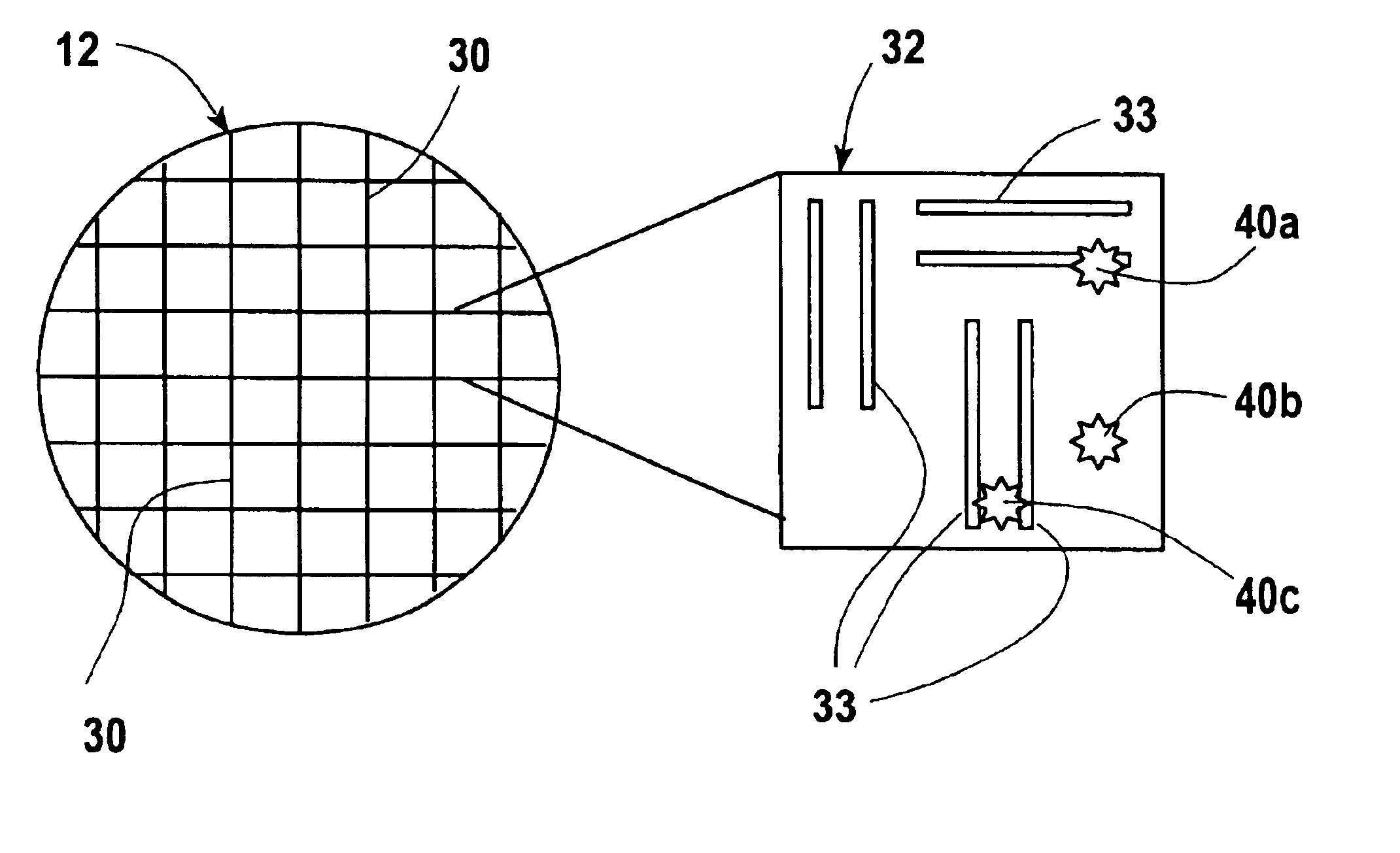
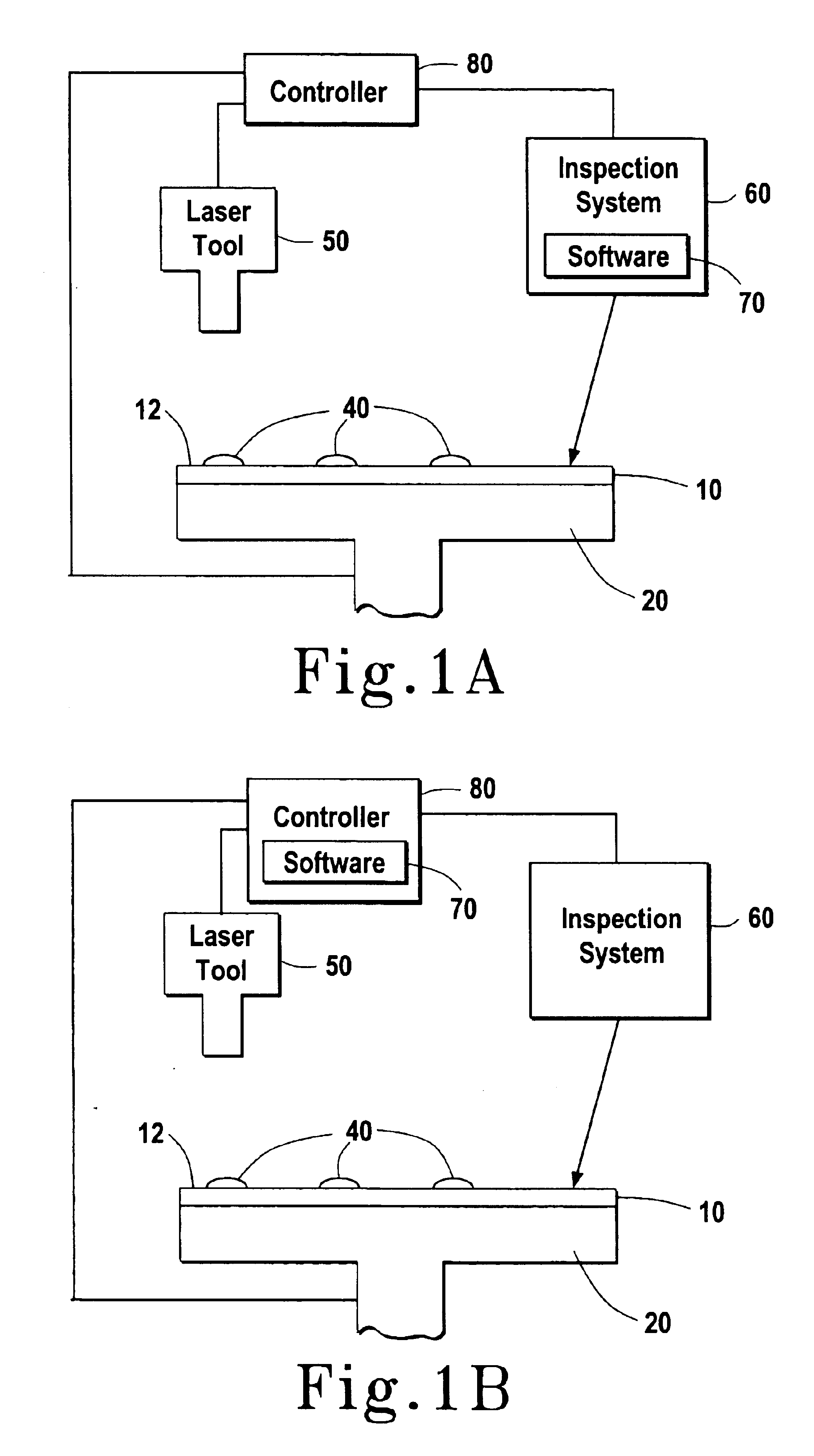
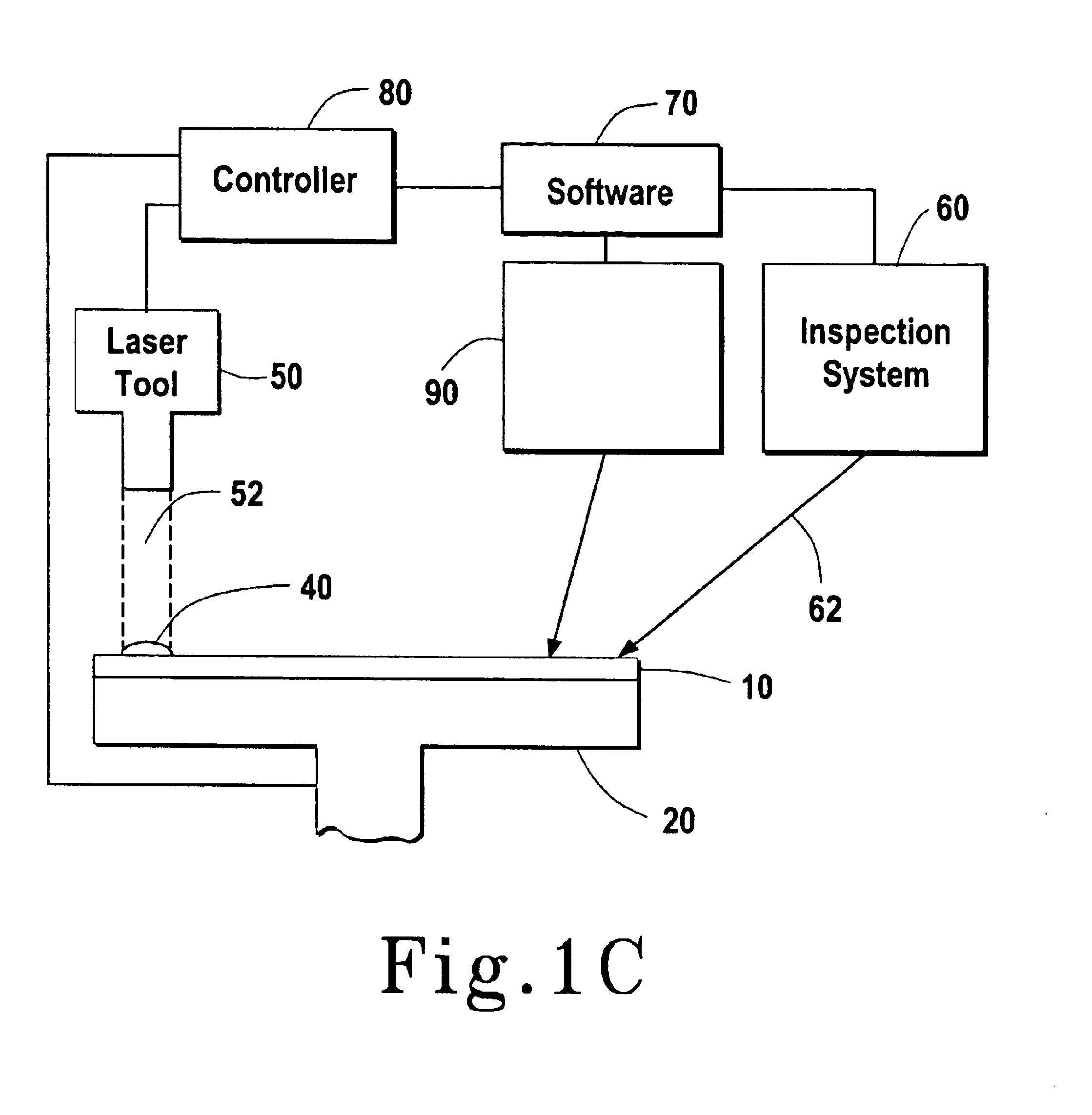
Likewise, if it is determined that the defect is an uncorrectable light point defect, it may also remain on the substrate surface.

