

Field emission electron source and production method thereof
a field emission and electron source technology, applied in the manufacture of electric discharge tubes/lamps, electrode systems, discharge tubes luminescnet screens, etc., can solve the problems of difficult to precisely fabricate a number of triangular pyramid shaped emitter chips, difficult to make their surface area larger, and complex manufacturing process of spindt type electrodes, so as to improve the electron emission characteristics and reliability of electron sources, reduce the barrier or high resistance layer between the semiconductor layer and the electrically conductive substrate, and improve the efficiency and reliability
- Summary
- Abstract
- Description
- Claims
- Application Information
AI Technical Summary
Benefits of technology
Problems solved by technology
Method used
Image

Examples
embodiment 1
(Embodiment 1)
Hereinafter, Embodiment 1 of the present invention will be described. In Embodiment 1, as an electrically conductive substrate (lower electrode), there is employed a single-crystalline n-type silicon substrate whose resistivity is comparatively close to a resistivity of a conductor (for example, a (100) substrate whose resistivity is 0.01 Ωcm to 0.02 Ωcm).
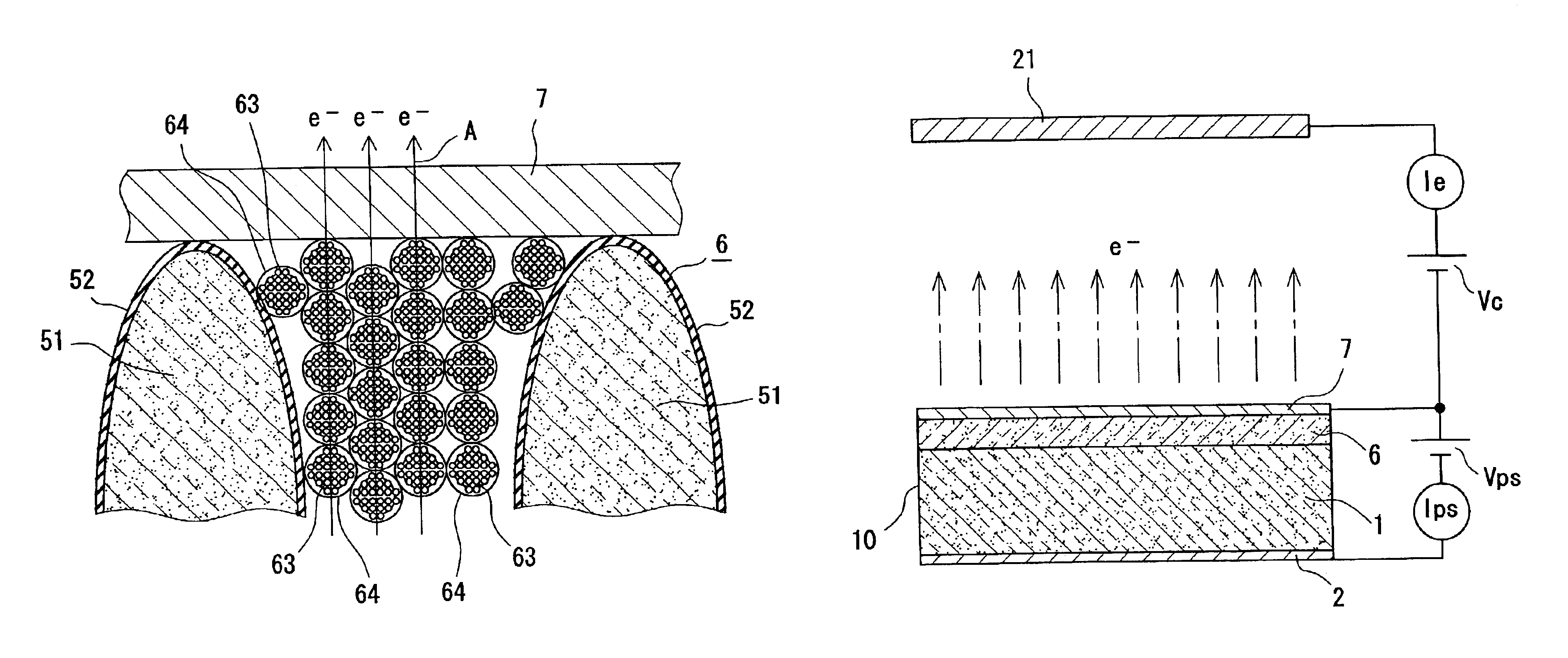
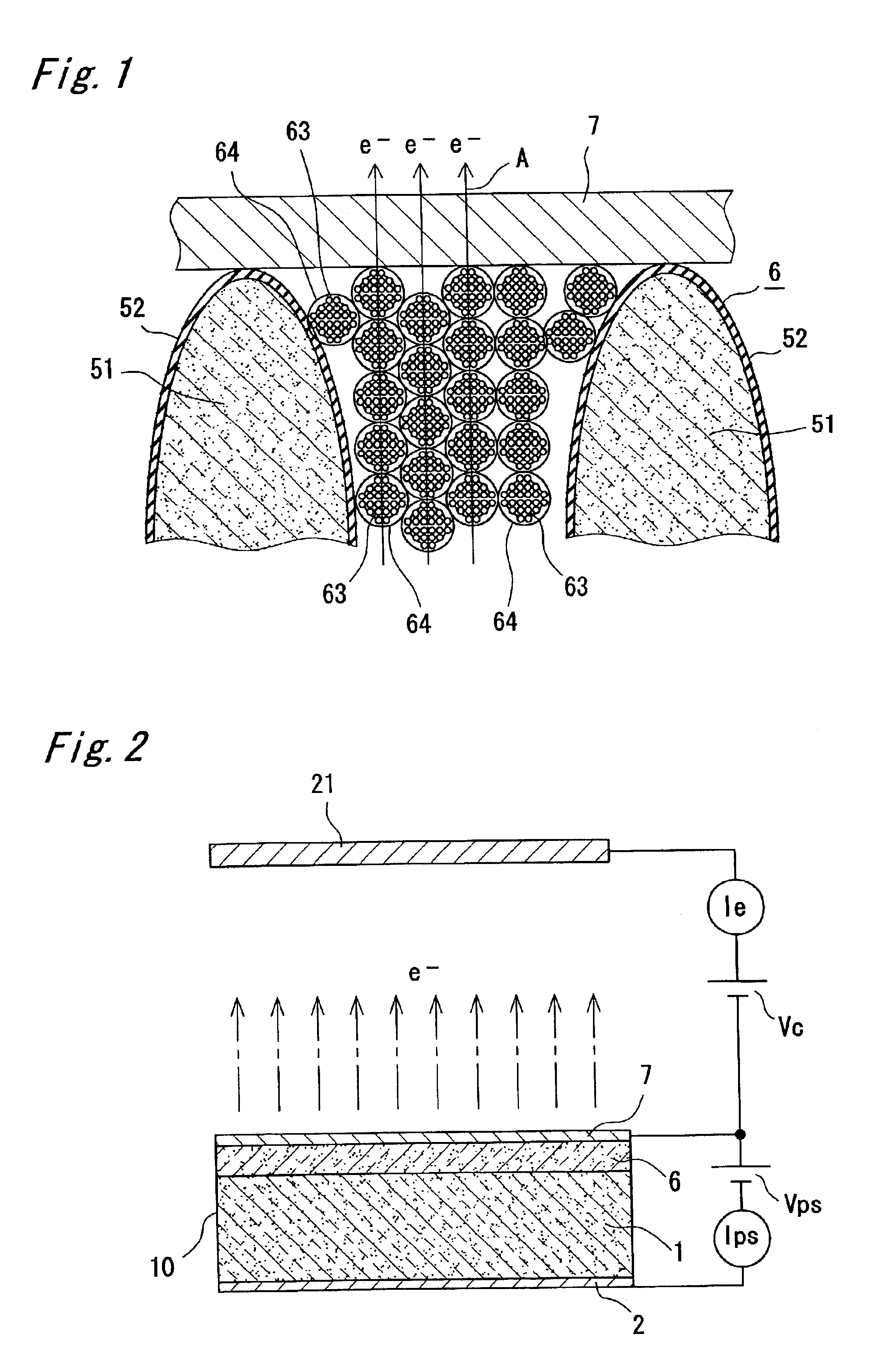
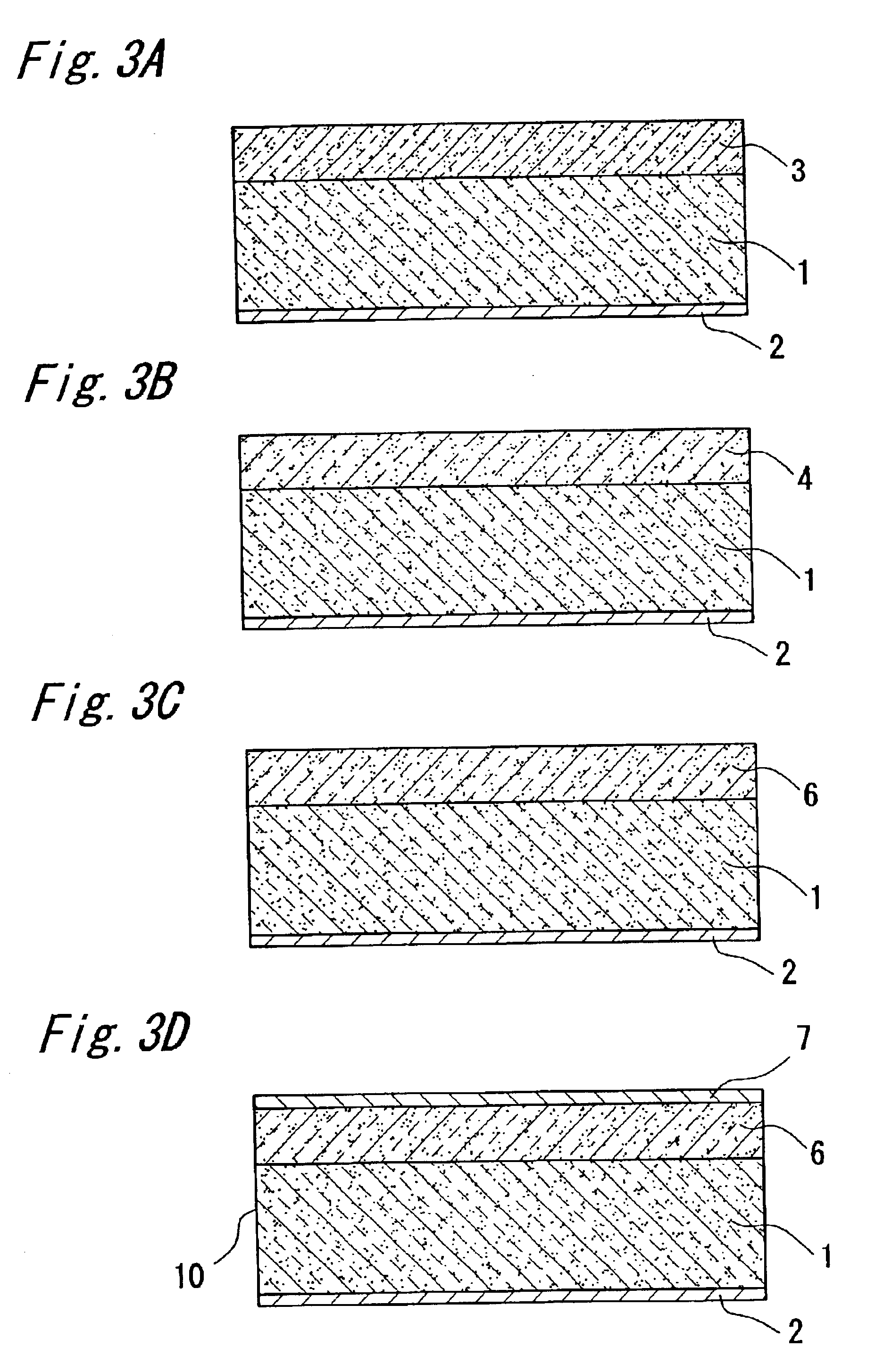
As shown in FIG. 2, in an electron source 10 (field emission-type electron source) according to Embodiment 1, a drift layer 6 (strong field drift layer) consisting of an oxidized porous polycrystalline silicon layer is formed on a main surface side of an n-type silicon substrate 1 that is an electrically conductive substrate. A surface electrode 7 is formed on the drift layer 6. An ohmic electrode 2 is formed on the back surface of the n-type silicon substrate 1. In Embodiment 1, the n-type silicon substrate 1 configures an electrically conductive substrate.
A material with its small work function is employed for a mat...
embodiment 2
(Embodiment 2)
Hereinafter, Embodiment 2 of the present invention will be described. In Embodiment 2, as an electrically conductive substrate, there is employed a substrate on which an electrically conductive layer consisting of a metal film (for example, tungsten film) is provided on one surface of an insulating substrate consisting of a glass substrate (for example, quartz glass substrate).
As shown in FIG. 11, in an electron source 10 according to Embodiment 2, a drift layer 6 consisting of an oxide porous polycrystalline silicon layer is formed on an electrically conductive layer 12 on an insulating substrate 11. A surface electrode 7 is formed on the drift layer 6. A configuration of the surface electrode 7 is similar to that of Embodiment 1.
In order to emit electrons from the electron source 10, a collector electrode 21 is arranged so as to be opposite to the surface electrode 7, and a vacuum state is established between the surface electrode 7 and the collector electrode 21. Th...
embodiment 3
(Embodiment 3)
Hereinafter, Embodiment 3 of the present invention will be described. An electron source according to Embodiment 3 has an insulating film consisting of a silicon oxide film. In Embodiment 3, as an electrically conductive substrate (lower electrode), there is employed a single-crystalline n-type silicon substrate whose resistivity is comparatively close to a resistivity of a conductor (for example, a (100) substrate whose resistivity is 0.01 Ωcm to 0.02 Ωcm).
As shown in FIG. 13, in an electron source 10 according to the embodiment 3, a drift layer 6 consisting of an oxidized porous polycrystalline silicon layer is formed on a main surface side of an n-type silicon substrate 1 that is an electrically conductive substrate. A surface electrode 7 is formed on the drift layer 6. An ohmic electrode 2 is formed on the back surface of the n-type silicon substrate 1. Therefore, a surface electrode 7 is opposed to a lower electrode 12, and the drift layer 6 is interposed between ...
PUM
 Abstract
Description
Claims
Application Information