

Photolytic conversion process to form patterned amorphous film
- Summary
- Abstract
- Description
- Claims
- Application Information
AI Technical Summary
Benefits of technology
Problems solved by technology
Method used
Image

Examples
example 1
Thin amorphous films of the complexes were deposited by spin coating onto silicon substrates. The complex Si(acac)2(O2CCH3)2 was dissolved in chloroform. This solution was spin coated on Si. A drop of the solution was dispensed onto a silicon chip spinning at 3000-rpm. The solvent evaporated leaving an amorphous film of the complex on the substrate. The optical quality thin film left on the surface was found to be 273 nm thick by optical interferometry. Fourier Transform Infrared (FTIR), and Ultraviolet-Visible (UV-Vis) Spectroscopy were used to confirm the presence of the film on the surface.
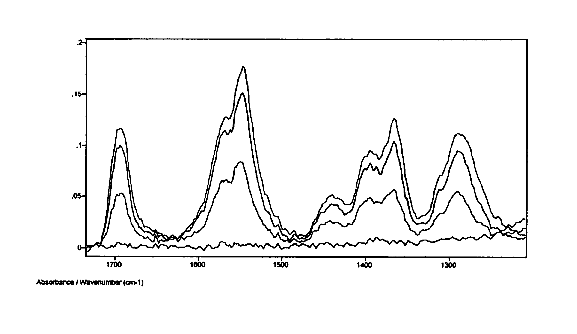
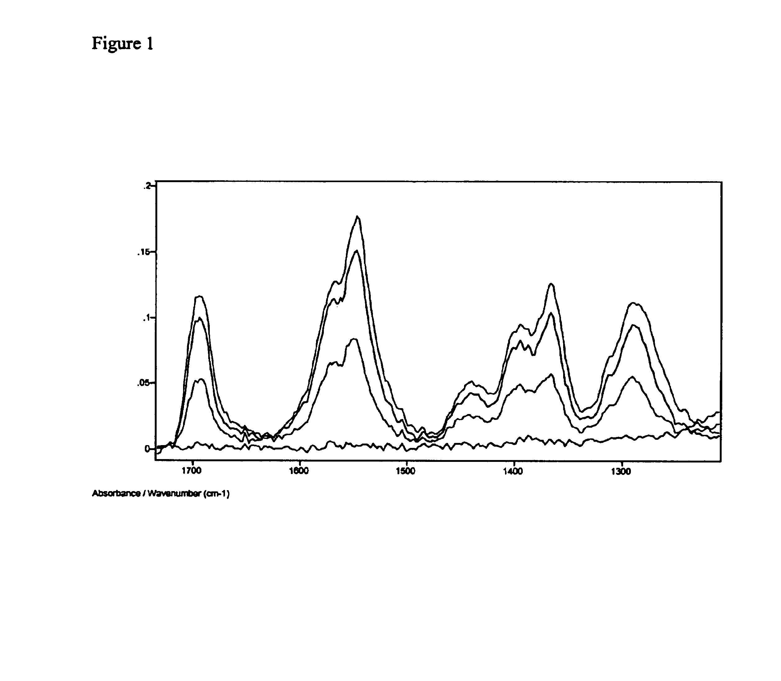
The FTIR spectrum of the film was recorded. The sample was then exposed to 254 nm light for one minute. A second spectrum was recorded. The process was repeated for several irradiation times until no vibration band due to the ligands was observed. The spectral changes in the FTIR during the photolysis experiment are showed in FIG. 1. Clearly, the vibration bands due to the ligands decrease in i...
example 2
A precursor Cu2(μ-Et2NCH2CH2O)2(N3)2 was deposited on a substrate. The Cu2(μ-Et2NCH2CH2O)2(N3)2 film was then photolyzed with ultraviolet light (254 nm) in a nitrogen atmosphere. The progress of the reaction was monitored by Fourier transform infrared spectroscopy. Following exhaustive photolysis, the conductivity of the film was measured. The films were found to have a conductivity of 1.8 μΩcm. The films were examined and found to consist of copper.
Alternatively, a similar precursor film exposed in air resulted in the formation of copper oxide. This oxide film could be reduced by hydrogen or any other suitable reductant at elevated temperatures to yield copper films.
example 3
A mixture of two precursors composed of both Cu2(μ-Et2NCH2CH2O)2(N3)2 and Cu2(μ-Et2NCH2CH2O)2(NCO)2 was deposited to form a film. This film was photolyzed to form a conductive copper based film.
In another embodiment, a film of Cu2(μ-Et2NCH2CH2O)2(N3)2 was deposited and photolyzed through a lithography mask. The resultant film was rinsed with ethylacetate and a copper oxide pattern remained on the surface.
PUM
| Property | Measurement | Unit |
|---|---|---|
| Temperature | aaaaa | aaaaa |
| Temperature | aaaaa | aaaaa |
| Temperature | aaaaa | aaaaa |
Abstract
Description
Claims
Application Information