III-V charge coupled device suitable for visible, near and far infra-red detection

a charge coupled, near-infra-red detection technology, applied in the direction of radiation control devices, solid-state devices, semiconductor devices, etc., can solve the problems of gate oxide sensitivity and other ways, limited si technology, gate oxide sensitivity to radiation flux, etc., to facilitate charge transfer, optimize drift velocity, and high field

Inactive Publication Date: 2005-03-22
UNIV OF CONNECTICUT
View PDF18 Cites 63 Cited by
  • Summary
  • Abstract
  • Description
  • Claims
  • Application Information

AI Technical Summary

Benefits of technology

[0013]A CCD epitaxial growth structure and fabrication technology have been invented which utilize a modulation doped interface to create an inversion channel for the storage of charge packets. The charge transfer is facilitated by the unique features of the epitaxial growth which include two delta-doped sheets of p type doping. One p type sheet is very close to the inversion channel and enables a resistive coupling between adjacent wells through a very thin sheet of highly doped material. The resistive coupling enables a high field and optimized drift velocity between pixels during the transfer phase which is responsible for the very high transfer rate. The second charge sheet positioned at the wafer surface enables a very low resistance ohmic contact to the gate metal contact. It is this ohmic contact that enables the HFET, which is the fundamental field effect device in the technology.

Problems solved by technology

Si technology is limited by the presence of the silicon oxide in both the active and passive regions of the integrated circuit in a number of ways.
A main limitation is the sensitivity of the oxide to radiation flux.
The radiation creates traps and other charged defects in the insulator which alter the internal voltage thresholds in both active and passive regions within the integrated circuit.
The gate oxide creates limitations in other ways as well.
Each overlapping gate creates a small region of thicker oxide between pixels which inhibits charge transfer and therefore sets a speed limitation upon the CCD.
These oxide barriers are fundamental to the Si CCD and constitute a transfer speed limitation.
However, these structures are then faced with barriers created by implant misalignment and a lack of well capacity.
A further limitation of the Si CCD is its spectral sensitivity.
It is also insensitive to UV radiation.
Two significant limitations of the QWIP as currently implemented are the existence of a significant level of dark current that necessitates cooling of the device to 77K and the fact that the device is not compatible with GaAs integrated circuits.
However, this compatibility has never been established and so present technology combines the GaAs QWIP wafer in a hybrid fashion with a Si read-out integrated circuit.
These technologies have always been plagued by the problem of low transfer efficiencies between pixels in the array.
The problem has been that no viable technique to implement resistive coupling has been found.
The use of deposited resistive layers was attempted but the resistive control problems discouraged further investigations.

Method used


Image

  • III-V charge coupled device suitable for visible, near and far infra-red detection
  • III-V charge coupled device suitable for visible, near and far infra-red detection
  • III-V charge coupled device suitable for visible, near and far infra-red detection

Examples


Embodiment Construction

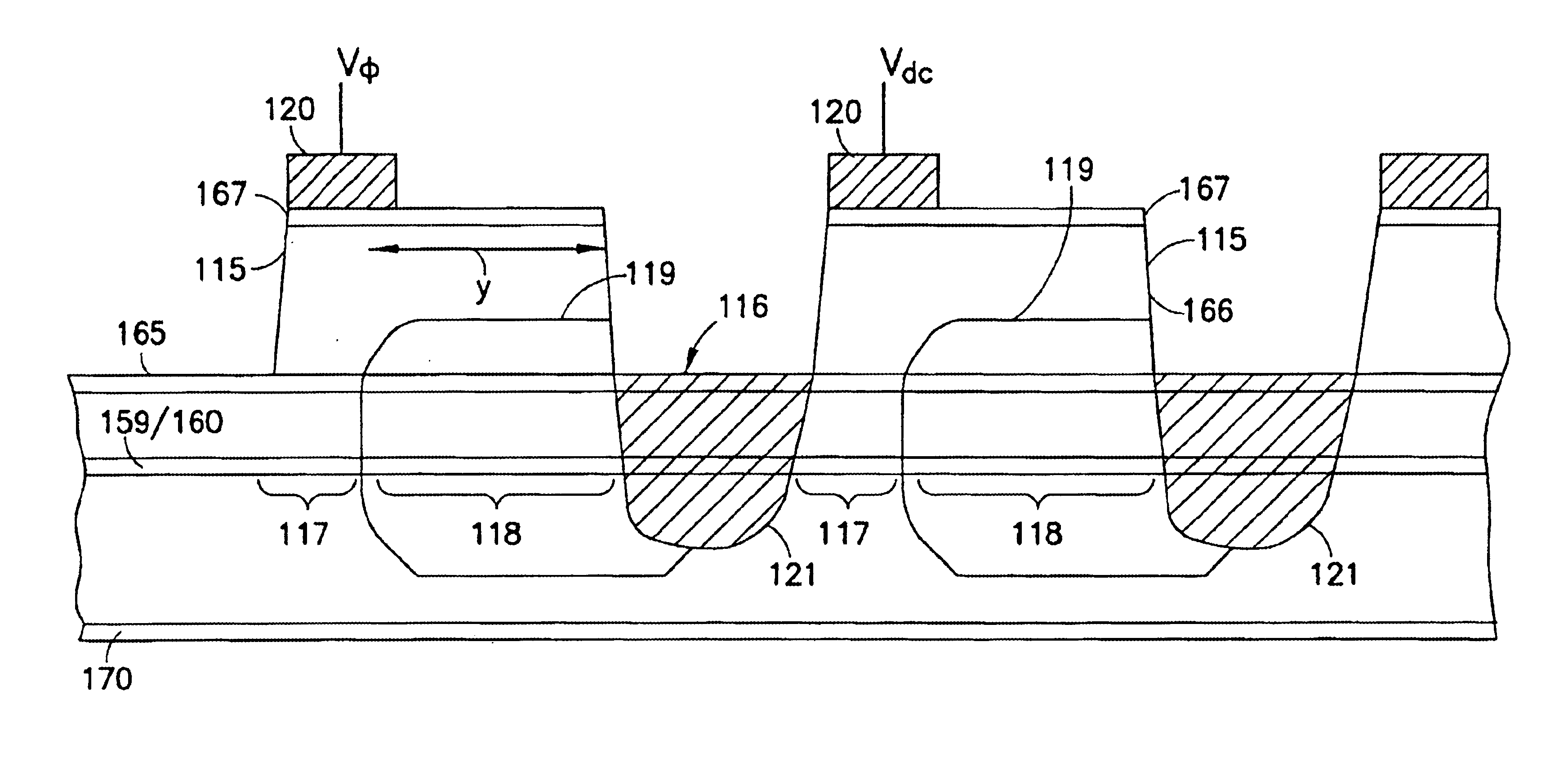
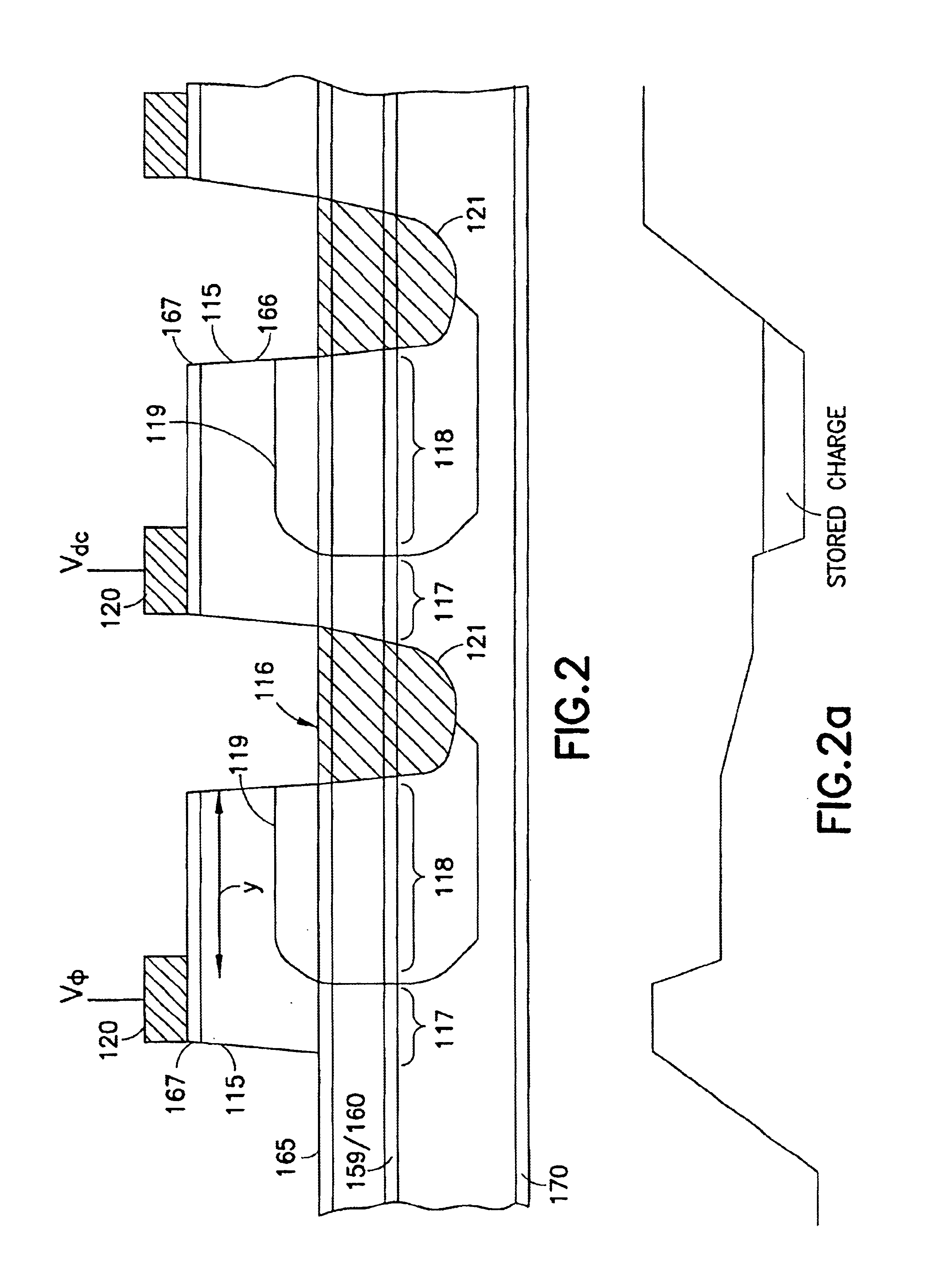
n showing all of the significant current flows from the contacts and into and out of the well.

[0021]FIG. 4 is a schematic drawing of the last pixel element in the CCD and its connection by way of a separate clocked output gate to the output differential amplifier by way of a floating diffusion node which is reset each clock cycle. For the active pixel architecture, Vφ is the single pixel element connected to the output amplifier stage.

DESCRIPTION OF THE PREFERRED EMBODIMENTS

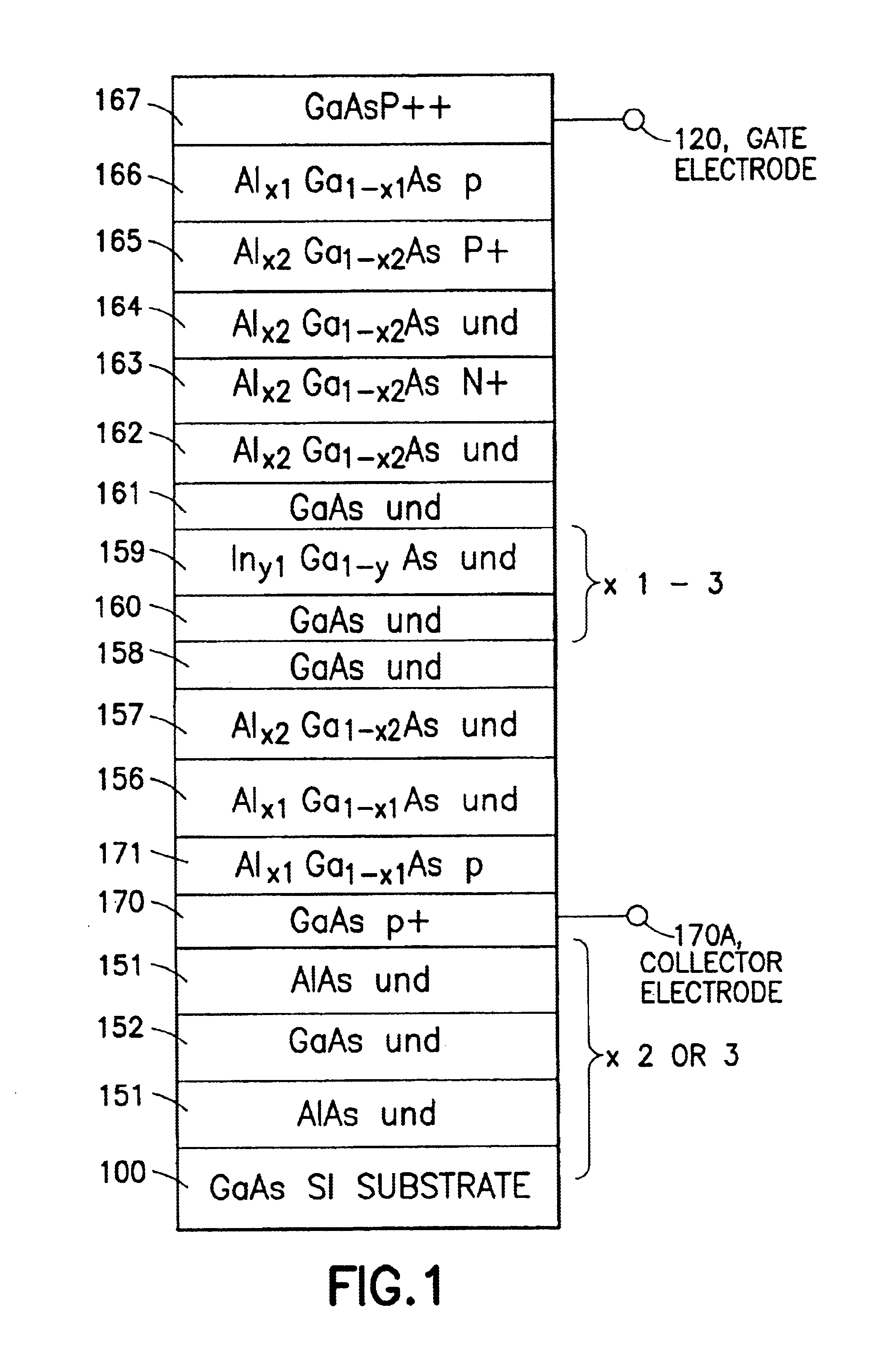
[0022]FIG. 1 shows the epitaxial layer structure corresponding to the preferred embodiment and from which the CCD, the active pixel and the HFET (heterostructure field effect transistor) can be made. The layer structure starts from a semi-insulating GaAs substrate 100 and grows a DBR (distributed Bragg reflector) mirror stack of 1-3 pairs of ¼ wavelength mirror using combinations of GaAs as layer 152 and AlAs as layers 151 which are subsequently oxidized to produce layers of AlxOy positioned between layers of GaA...


PUM


Abstract

A photon detector is obtained by using the intersubband absorption mechanism in a modulation doped quantum well(s). The modulation doping creates a very high electric field in the well which enables absorption of input TE polarized light and also conducts the carriers emitted from the well into the modulation doped layer from where they may recombine with carriers from the gate contact. Carriers are resupplied to the well by the generation of electrons across the energy gap of the quantum well material. The absorption is enhanced by the use of a resonant cavity in which the quantum well(s) are placed. The absorption and emission from the well creates a deficiency of charge in the quantum well proportional to the intensity of the input photon signal. The quantity of charge in the quantum well of each detector is converted to an output voltage by transferring the charge to the gate of an output amplifier. The detectors are arranged in the form of a 2D array with an output amplifier associated with the entire array or a row of the array as in the known charge coupled devices, or a separate amplifier could be dedicated to each pixel as in the known architecture of the active pixel device. This detector has the unique advantage of near room temperature operation because the dark current is limited to the generation across the semiconductor bandgap and not the emission over the quantum well barrier. The detector also has the advantage that the readout circuitry is implemented monolithically by the HFETs formed in the GaAs substrate simultaneously, with the detecting elements.

Description

TECHNICAL FIELD OF THE INVENTION[0002]This invention relates to the field of charge coupled and active pixel image sensors that are fabricated in the III-V material systems and have sensitivities over a broad spectral range including the UV, visible, near and far infrared regions.BACKGROUND OF INVENTION[0003]Next generation imaging systems are required to have Charged Coupled Devices (CCD's) that operate at very high frequencies and to have a high resistance to radiation flux (the imager is said to be radiation hardened). Many of these applications are in space where radiation flux is significant and reliability is critical. State-of-the-art imagers are constructed as Si integrated circuits in the form of CCD's or active pixel arrays. In the CCD, the pixels are clocked sequentially to a common output amplifier. In the active pixel array, the array is x-y addressable and each pixel is output to its own dedicated amplifier (the array is output on a row by row or column by column basis...

Claims


Application Information

Patent Timeline
Patent Type & Authority Patents(United States)
IPC IPC(8): H01L27/146H01L27/148H01L31/0304H01L31/0352
CPCB82Y20/00H01L27/14652H01L31/0304H01L31/035236H01L27/14806Y02E10/544
Inventor TAYLOR, GEOFF W
Owner UNIV OF CONNECTICUT
Why Eureka
Try Eureka