Systems and methods for forming refractory metal nitride layers using organic amines

a technology of organic amines and refractory metals, applied in the direction of coatings, chemical vapor deposition coatings, capacitors, etc., can solve the problems of frequent formation of undesirable interfacial layers of siosub>2 /sub>, high leakage paths and channels, and dielectric layers approaching only 10 in thickness, so as to minimize the effect of detrimental gas phase reaction and improved layer thickness control

Inactive Publication Date: 2005-11-22
MICRON TECH INC
View PDF39 Cites 148 Cited by
  • Summary
  • Abstract
  • Description
  • Claims
  • Application Information

AI Technical Summary

Benefits of technology

[0023]“Barrier layer” as used herein refers to a conductive, interfacial layer that can reduce diffusion of ambient oxygen through a dielectric layer into a semiconductor substrate (typically a polysilicon substrate) or can reduce diffusion of one layer into another, such as a copper conductive layer into a semiconductor substrate (typically a polysilicon substrate). For this invention, the barrier layer is a tantalum nitride or tantalum silicon nitride layer.
[0028]“Atomic layer deposition” (ALD) as used herein refers to a vapor deposition process in which numerous consecutive deposition cycles are conducted in a deposition chamber. Typically, during each cycle the metal precursor is chemisorbed to the substrate surface; excess precursor is purged out; a subsequent precursor and / or reaction gas is introduced to react with the chemisorbed layer; and excess reaction gas (if used) and by-products are removed. As compared to the one cycle chemical vapor deposition (CVD) process, the longer duration multi-cycle ALD process allows for improved control of layer thickness by self-limiting layer growth and minimizing detrimental gas phase reactions by separation of the reaction components. The term “atomic layer deposition” as used herein is also meant to include the related terms “atomic layer epitaxy” (ALE) (see U.S. Pat. No. 5,256,244 (Ackerman)), molecular beam epitaxy (MBE), gas source MBE, organometallic MBE, and chemical beam epitaxy when performed with alternating pulses of precursor compound(s), reaction gas and purge (i.e., inert carrier) gas.

Problems solved by technology

However, the continuous shrinkage of microelectronic devices over the years has led to dielectric layers approaching only 10 Å in thickness (corresponding to 4 or 5 molecules).
However, these metal-containing layers can provide high leakage paths and channels for oxygen diffusion, especially during annealing.
Also, an undesirable interfacial layer of SiO2 is frequently created by oxidation of polysilicon during the annealing of the dielectric layer.
This copper diffusion has led to degradation of device reliability, causing semiconductor manufacturers to turn toward other less conductive metals, such as aluminum and tungsten.
However, when PVD methods are used, the stoichiometric composition of the formed metal nitride and metal silicon nitride barrier layers such as Ta—N and Ta—Si—N can be non-uniform across the substrate surface due to different sputter yields of Ta, Si, and N. Due to the resulting poor layer conformality, defects such as pinholes often occur in such layers creating pathways to diffusion.

Method used


Image

  • Systems and methods for forming refractory metal nitride layers using organic amines
  • Systems and methods for forming refractory metal nitride layers using organic amines
  • Systems and methods for forming refractory metal nitride layers using organic amines

Examples


example 1

Pulsed CVD of TaN Using TaF5 and HN(SiHMe2)2.

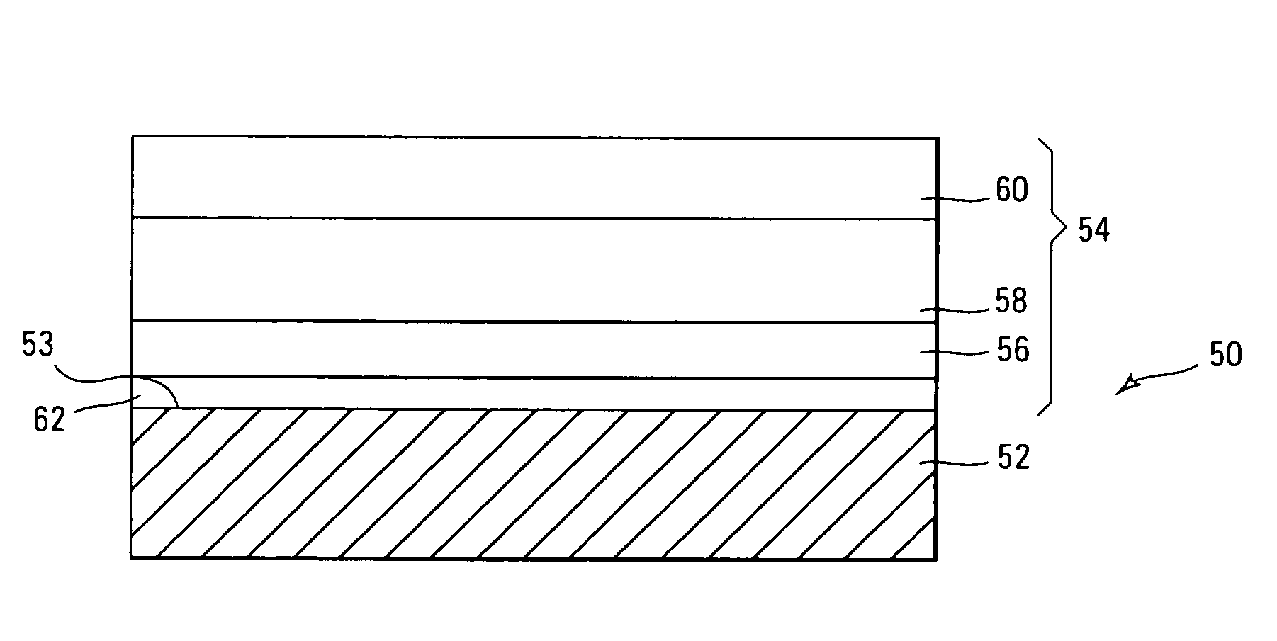
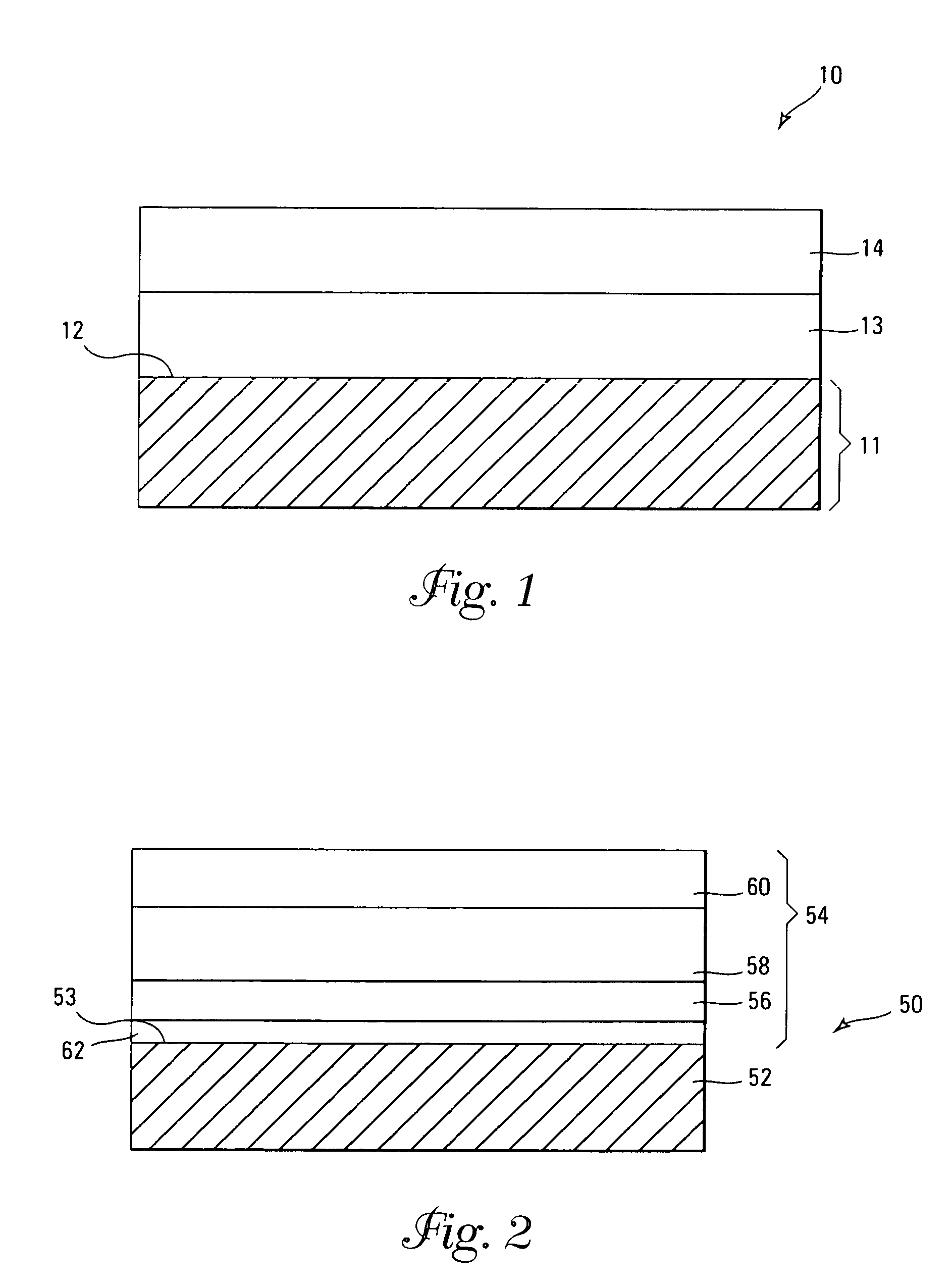
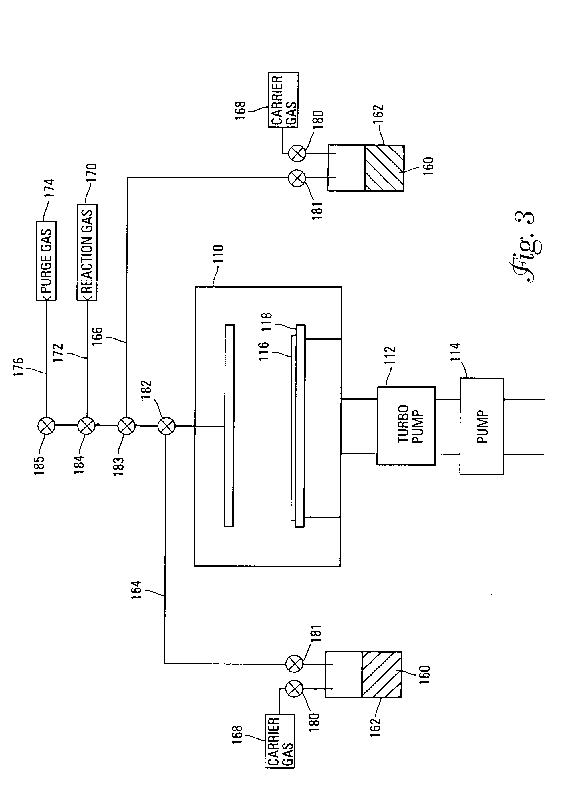
[0069]A chamber of configuration shown in FIG. 3 was set up with pneumatic valves under computer control to pulse the valves open in sequential manner. Two reservoirs connected to the chamber contained TaF5 (Alfa Aesar, Ward Hill, Mass.) and tetramethyldisilazane (TMDS) (Sigma-Aldrich Chemical C., Milwaukee, Wis.). The TaF5 reservoir was held at 75° C. and the TMDS at ambient. The substrate was a silicon wafer having borophosphosilicate glass (BPSG) as a top layer and was maintained at 255° C. for the deposition.

[0070]Each cycle involved a 2-second pulse of TaF5 and a 1-second pulse of TMDS, each separated by a 1-second purge with argon and a 2-second pump down under dynamic vacuum. The precursors were introduced without carrier gases, using only a mass flow controller for the TMDS vapor, set at 100 sccm. After 300 cycles a TaN film 110 nm thick was obtained, having a resistivity of 7150 μΩ-cm as measured using a four-point probe. The fil...


PUM

PropertyMeasurementUnit
adsorption energiesaaaaaaaaaa
deposition temperaturesaaaaaaaaaa
temperatureaaaaaaaaaa

Abstract

A method of forming (and apparatus for forming) refractory metal nitride layers (including silicon nitride layers), such as a tantalum nitride barrier layer, on a substrate by using an atomic layer deposition process (a vapor deposition process that includes a plurality of deposition cycles) with a refractory metal precursor compound, an organic amine, and an optional silicon precursor compound.

Description

FIELD OF THE INVENTION[0001]This invention relates to methods of forming refractory metal nitride layers (including silicon nitride layers) on substrates using a vapor deposition process, particularly a multi-step atomic layer deposition process, with a refractory metal precursor compound, an organic amine, and optionally a silicon precursor compound. The formed refractory metal (silicon) nitride layers are particularly useful as diffusion barriers for polysilicon substrates to reduce diffusion of oxygen, copper, or silicon.BACKGROUND OF THE INVENTION[0002]In integrated circuit manufacturing, microelectronic devices such as capacitors are the basic energy storage devices in random access memory devices, such as dynamic random access memory (DRAM) devices, static random access memory (SRAM) devices, and ferroelectric memory (FERAM) devices. Capacitors typically consist of two conductors acting as electrodes, such as parallel metal (e.g., platinum) or polysilicon plates, that are insu...

Claims


Application Information

Patent Timeline
Patent Type & Authority Patents(United States)
IPC IPC(8): C23C16/34H01L21/285H01L21/70H01L21/02H01L21/768C23C16/44C23C16/455
CPCC23C16/34C23C16/45523C23C16/45553H01L21/28562H01L21/3141H01L21/31637H01L21/76841H01L21/76843H01L28/57H01L21/0228H01L21/02183
Inventor VAARTSTRA, BRIAN A.
Owner MICRON TECH INC
Why Eureka
Try Eureka