[0016]The design of the ASIC is guided by two principal goals. The first goal was to make the chip applicable to as wide a variety of applications as possible; this called for a flexible yet easy to use design. It has the ability to combine, on the same chip, signals that differ in terms of their polarity,
rise time, threshold requirements, etc. This option, which is not available on the present RENA chip, enables users to optimize their
system layout for the shortest possible
signal connections, without regard to
signal type. This contributed to achieving the second goal, which is equal in importance to the first, namely performance, for example, to obtain the best resolution possible for the combined
detector-readout
system. To reach this goal, we have designed the RENA-2 ASIC to achieve the lowest possible
noise consistent with the characteristics of the detectors with which the ASIC is intended to be used.
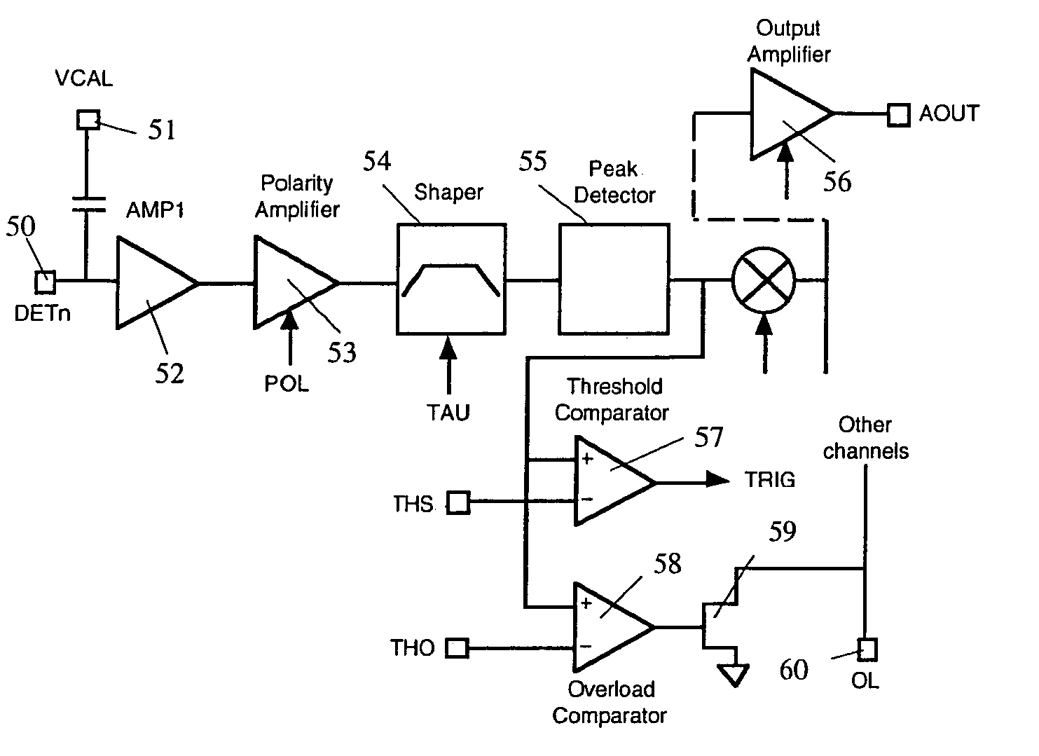
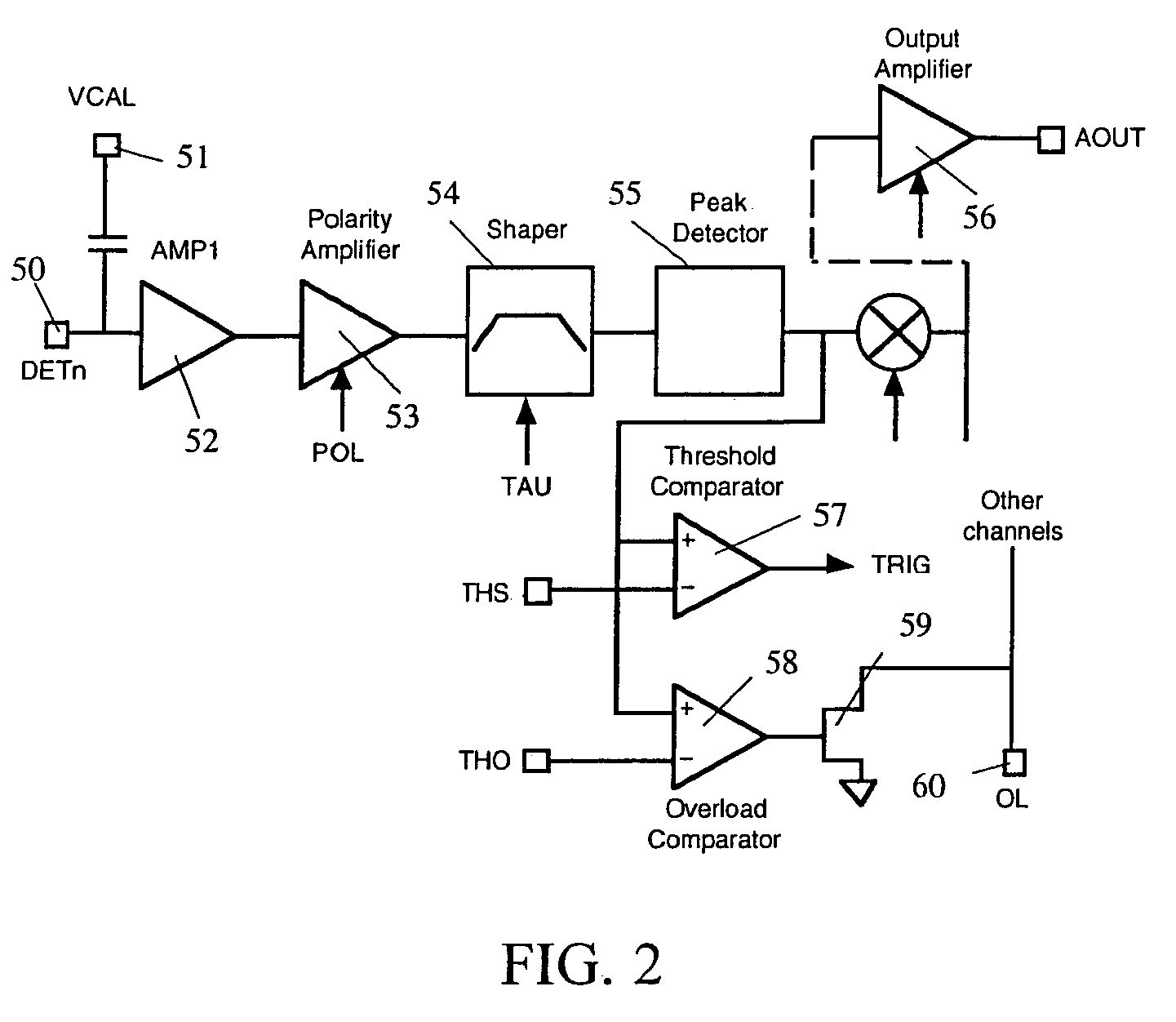
[0018]The features include low-
noise performance, self-trigger capability, several different peaking times, different readout
modes, and the daisy-chain option. New innovative features, such as user-selectable dynamic ranges and the ability to provide channel-by-channel timing information, were added. These new features, as well as the significant performance improvements required a completely new design for the new developed ASIC. The design goal for the
noise performance, in particular, represents a significant improvement over the present RENA chip and substantial innovation was required in order to reach this goal. Innovation was even more urgently needed to achieve improved noise performance while reducing the chip's
power consumption.
[0020]Table I shows the main specifications for RENA-2 ASICs. These features include the chip's low-noise performance, its self-trigger capability, and the versatility it offers by providing several different peaking times, different readout
modes, and the daisy-chain option. New, innovative features include
low noise, self resetting charge sensitive
input amplifier, selectable multi-range shaper, user-selectable dynamic ranges, fast trigger output for coincident event detection and the ability to provide channel-by-channel
time difference information. The
comparator thresholds will be individually adjustable through an 8 bit DAC on each channel. This will allow accurate and uniform threshold setting throughout the
detector. Two very important new features for space deployment are the adjustable
power consumption by limiting the current flow to the input
transistor and the
radiation hardness inherent to the 0.5 micron
CMOS process. The peaking times were made adjustable from about 0.4 to 40 microseconds, which makes the chip suitable for a wide range of detectors, from CdZnTe to HgI2 as listed above. The new chip incorporates a pole zero cancellation circuit to
handle large rates without significant pileup. The functionality of the new RENA ASIC is dramatically improved by eliminating unnecessary connections and interface. Another important new feature is the inclusion of 4 extra channels to allow the connection of the
cathode side into the same ASIC. The
input amplifier is made tolerant to leakage current so that the ASIC can be used DC coupled which eliminates the need to use
capacitive coupling.
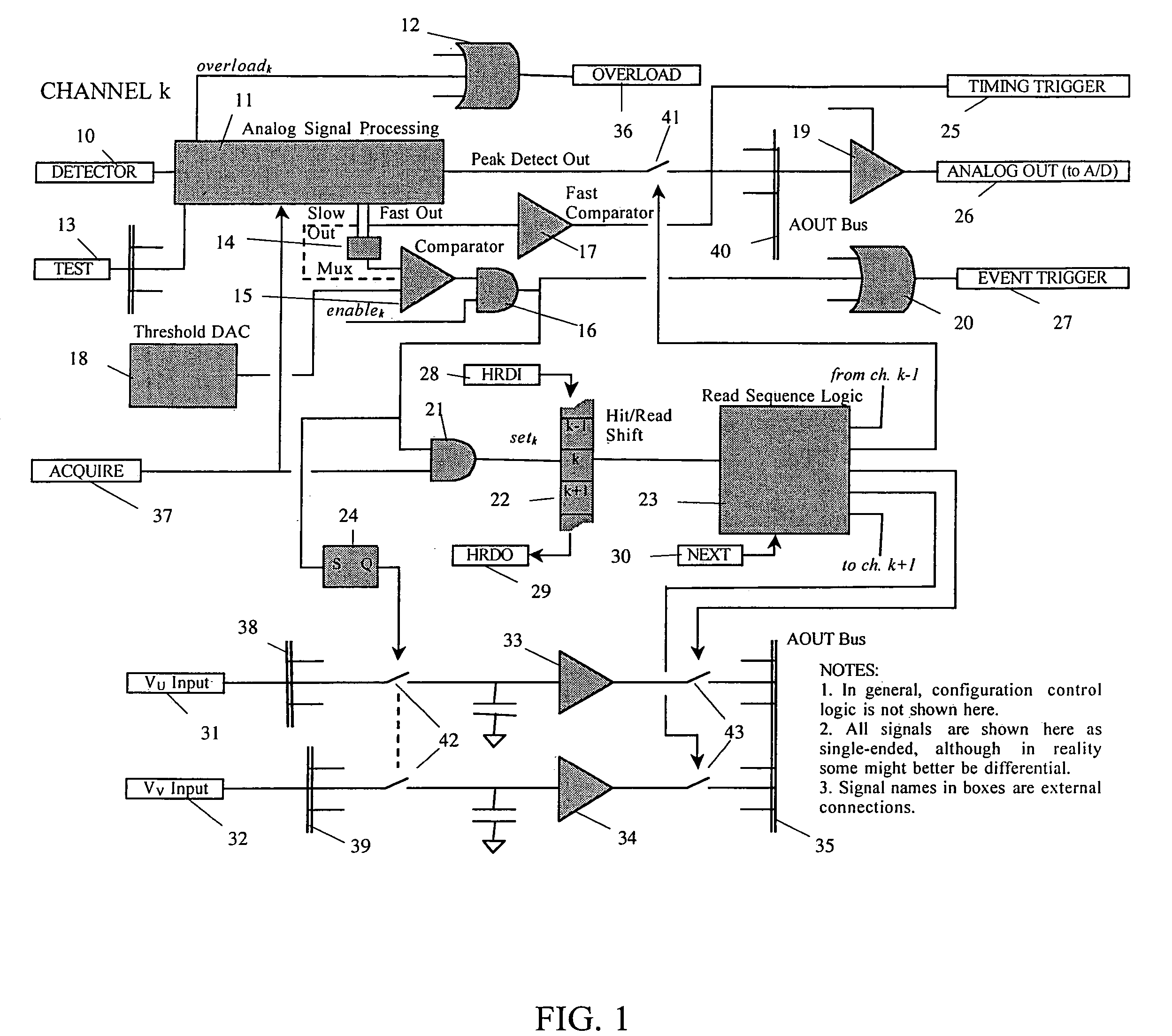
[0021]The RENA chip offers the user some flexibility by providing a variety of readout modes—sparse, nearest neighbor, and global readout. The nearest neighbor mode is quite useful to account for
charge sharing in strip detectors or other essentially one-dimensional detector arrays. However, its successful application requires a monotonic mapping of detector strips to RENA channels, which is not always optimal from the point of view of interconnect
capacitance or mechanical constraints. In addition, extension of the nearest neighbor mode to two-dimensional arrays, though equally desirable, is not possible, simply because there is no “natural” mapping from the four to eight nearest neighbors of a given pixel to the sequence of channels on the readout chip. Instead, RENA-2 provides the user with high flexibility that is the ability to specify which channels are to be read on a case-by-case basis. In this
scenario, the readout pattern is controlled by a serial
shift register with one bit per channel; if a bit is set, the corresponding channel is read out. Initially, when a channel triggers, the corresponding bit in the readout register is set. Before reading out the detector data, the
control logic can inspect the trigger pattern and, if necessary, replace it with a different readout pattern. This operation can be completed in 2.3 μs (for 36 channel ASIC), regardless of the total system channel count, with a suitably designed external controller FPGA; it need not significantly compromise the
dead time specification. The readout pattern can be a nearest neighbor pattern customized to the particular experimental setup. This gives significant flexibility for application to a variety of detectors of different configurations such as pixel and strip detectors.

