Multilayer microcavity devices and methods

a microcavity and multi-layer technology, applied in the field of microelectrodes, can solve the problems of constructing electrodes with dimensions smaller than 1 m, unable to address the formation of small cavities or the placement of probes, and unable to achieve the effect of detecting in a fast time scal

Inactive Publication Date: 2006-12-05
SMITHKLINE BECKMAN CORP +1
View PDF46 Cites 67 Cited by
  • Summary
  • Abstract
  • Description
  • Claims
  • Application Information

AI Technical Summary

Benefits of technology

[0024]Any of the electrodes in the cavities or pores may be modified and used as reference electrodes or working electrodes, allowing complete electrochemical experiments to be performed within the cavity.
[0082]Another object of the invention is to provide a microcavity device for rapid detection and analysis of an analyte in the microcavity.

Problems solved by technology

This is motivated by the cost, availability and toxicity of the samples tested or monitored as well as that of the materials used to make the cells.
Many problems are associated with the materials used to make and modify them.
Unfortunately, such an approach does not address formation of small cavities or placement of probes, such as electrodes, both inside and outside so that both compartments on either side of the film can be analyzed.
Despite the advantages of microelectrodes, progress has been impaired by difficulty in constructing electrodes with dimensions smaller than 1 μm.
The grinding process has been shown to be less reproducible and leads to significantly smaller limiting currents.
However, the electrodes on the array were not independently addressable.
However, because they are extremely thin, they are flimsy and tear easily unless they are well supported.
However, two major problems that are inherent in constructing such a device are the need for a high degree of control over spatial distribution of the materials and a means by which to probe the array.
Disadvantages include denaturation of the molecules due to the attachment procedure, difficulties in controlling the environment around the molecules either because the molecules are directly on the surface or because the surrounding molecular network is not very well ordered, and a lack of reliability in the results due to the proximity of the membrane and the electrode.
There is also the problem of the effect of the substrate on the properties of the film and the permeability of the film.
These significant problems call into serious question the accuracy of measurements obtained using these techniques.
This limits the analytical applications to systems that exhibit a change in the conductance through the membrane.
The first two tools pose two significant disadvantages; the pinhole or pipet tip is too small for convenient spectroscopic analysis and the distance between membrane and electrodes (for conductivity measurements) is limited to large values (millimeters or greater).
In both cases, electrodes on either side of the bi-layer are macroscopic in size an cannot be positioned close enough to the bi-layers to monitor diffusion.
In fact, these techniques only monitor capacitance of the bi-layers or changes in conductivity of ions through them, where electrodes do not need to be located adjacent to the bi-layers.
They are incapable of accurately measuring diffusion or transport across the membranes.
However, it is not useful for studies of assembly dynamics or conductivity measurements.
A problem with most encapsulants is the limited control available for dispensing the contents.

Method used


Image

  • Multilayer microcavity devices and methods
  • Multilayer microcavity devices and methods
  • Multilayer microcavity devices and methods

Examples


example 1

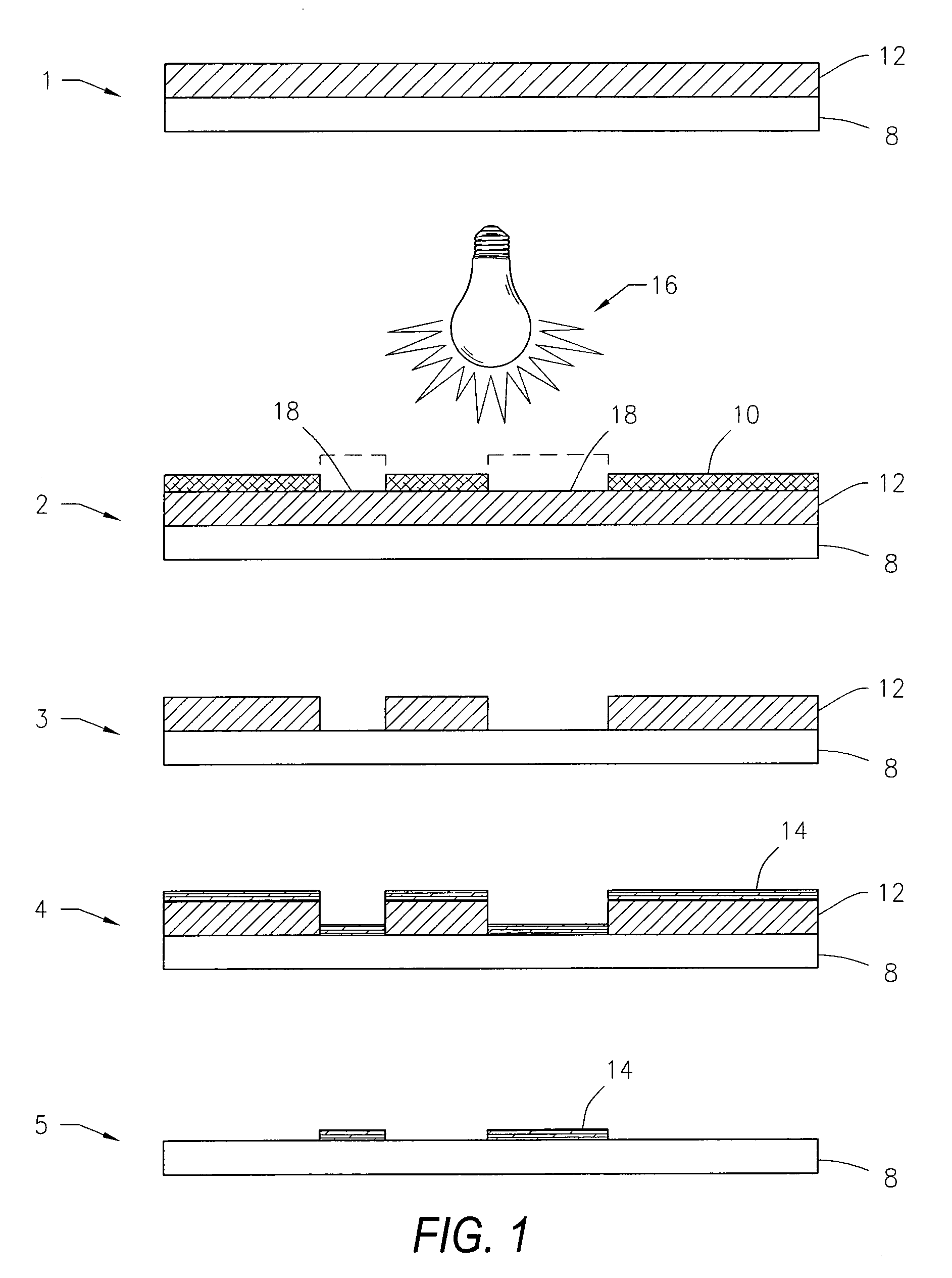
[0152]Microfabricated recessed microdisk electrodes (RMDs) of 14 and 55 μm diameter were constructed. For evaluation of electrode function, both faradaic current in Ru(NH3)63+ solution and charging current in KNO3 solution were measured with cyclic voltammetry (CV). At slow scan rates (0.1 Vs−1), where radial diffusion dominates, the steady state measured with 55 μm RMD is 53.5±0.48 nA and the 14 μm RMD is 5.39±0.96 nA. At fast scan rates (204 Vs−1), where linear diffusion dominates, the current measured with the 55 μm RMD is 784.6±42.0 nA and the 14 μm RMD is 35.4±9.5 nA. The dependence of capacitance on scan rate of the RMDs was found to be similar to that of a macroelectrode, indicating good adhesion between the insulator and the electrode. The signal-to-noise ratio of the RMD compared to a planar disk microelectrode (PDM) is on average 4 times greater for both of the stirred solutions.

[0153]All chemicals are reagent grade and used as received. Aqueous solutions are prepared with...

example 2

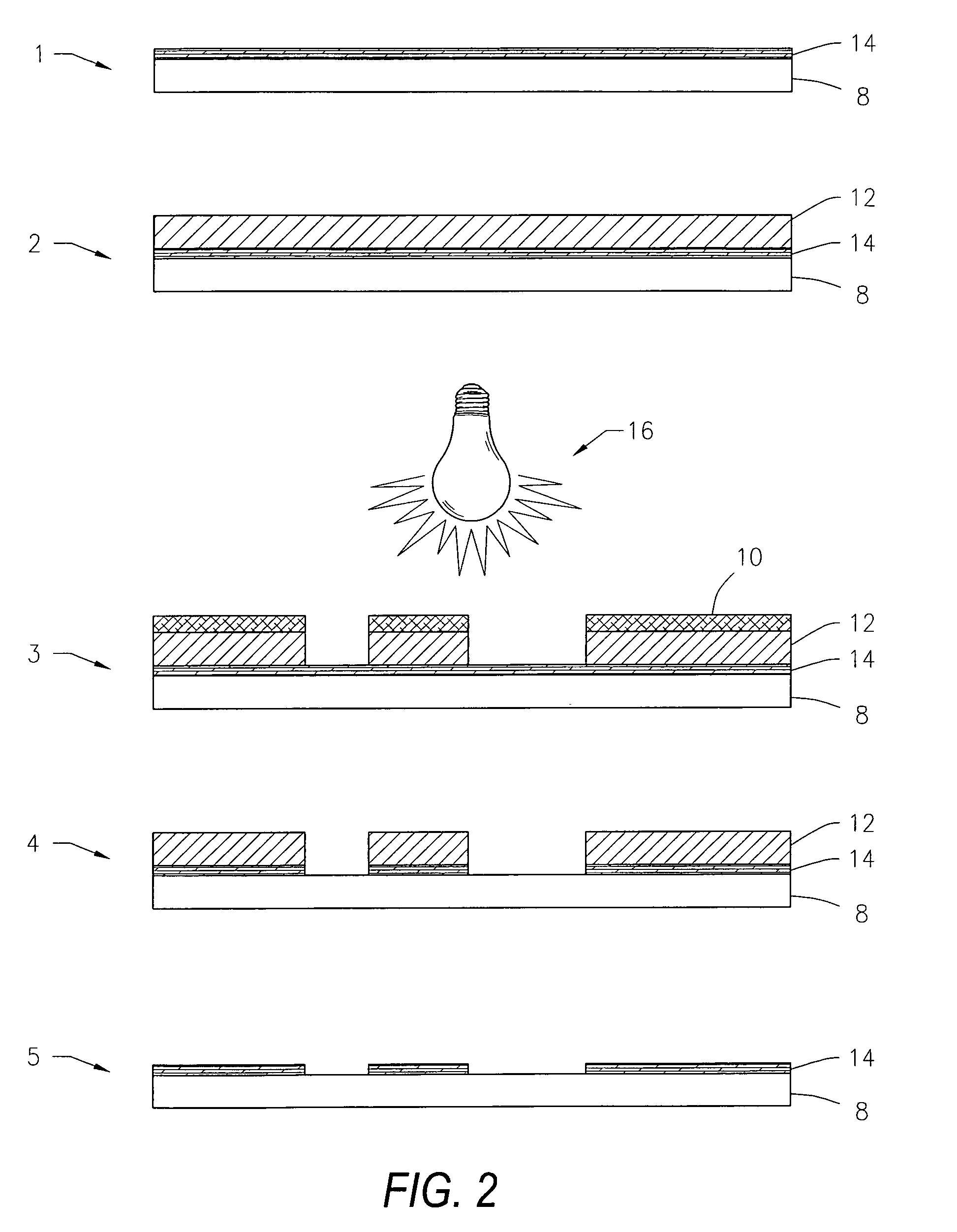
[0165]Construction and characterization of an electrochemical cell containing two individually-addressable microelectrodes, a disk and a nanoband are described. The diameter of the cell is 53 μm and the depth 8 μm. The RMD and TNE separated vertically by 4 μm. Both electrodes are evaluated using cyclic voltammetry in Ru(NH3)63+ and electrolyte. The faradaic response is compared with theories for radial and linear diffusion for both geometries. The response of the recessed disk microelectrodes (RMD) is compared to previous work211 to evaluate the effects of depth of the response. Capacitance as a function of scan rate for both microelectrodes is compared to a macroelectrode to determine the quality of construction.

[0166]All chemicals are reagent grade and used as received. Aqueous solutions are prepared with high purity deionized water (Milli-Q). A gold coin (Credit Suisse, 99.99%) and chromium plated tungsten rod (R. D. Mathis) served as sources for thermal evaporation. Silicon wafe...

example 3

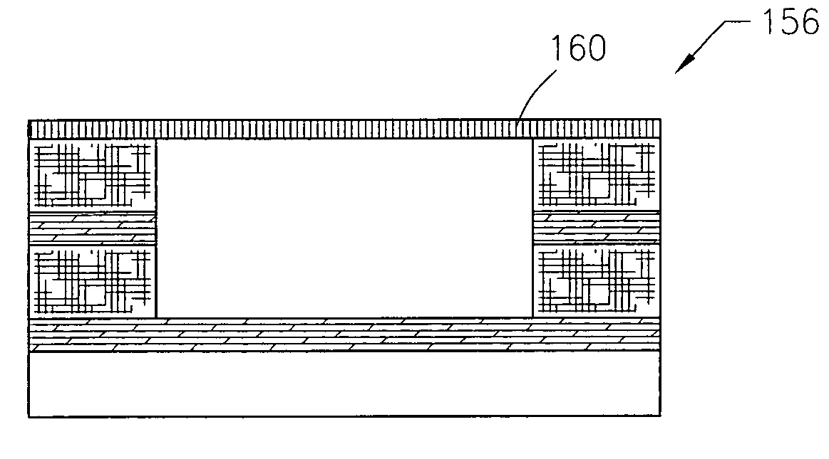
[0178]This example illustrates how microcavities may be modified in order to form troughs having electrodes on either side. They retain the small dimensions regarding height and width, but have macroscopic length.

[0179]All reagents (Aldrich) were reagent grade and were used without further purification, unless otherwise specified. Deionized (DI) water was prepared using an ultrapure water system (Millipore, France model Milli Q RG). Sulfuric acid, hydrogen peroxide, iso-propanol were electronic grade (J. T. Baker). A cold coin (Canadian Maple Leaf, 99.9%) and chromium-plated tungsten rods (R. D. Mathis) were used as sources for thermal evaporation. For photolithography, HR 200 negative photoresist, WNRD negative resist developer, PF thinner and universal photoresist stripper Nophenol (OCG Microelectronic Materials, Inc.) were used.

[0180]Deposition of Chromium, Gold and Silicon Nitride. Glass slides (Fisher Scientific) were cut to 1 in.×1 in. and cleaned with a 7:3 (v / v) solution of ...


PUM

PropertyMeasurementUnit
heightaaaaaaaaaa
diameteraaaaaaaaaa
volumeaaaaaaaaaa

Abstract

Microcavities and micropores that are microscopic (<1 mm) in width and depth and contain any number of individually-addressable electrodes, separated by insulators, along the walls of each cavity. The conducting materials, and the insulator materials can be deposited alternately onto a starting substrate, which is typically an oxidized silicon wafer or polyimide film, but may be any substrate that shows good adhesion to the materials layered on it. The cavities are etched through these layers, perpendicular to the plane of the substrate, exposing the layers at their edges. Pores may be carved entirely through the device.

Description

CROSS-REFERENCE TO RELATED APPLICATIONS[0001]This application is a continuation-in-part of U.S. patent application Ser. No. 09 / 775,937, filed Feb. 2, 2001, abandoned, which is a continuation-in-part of U.S. patent application Ser. No. 09 / 255,950 filed Feb. 23, 1999, abandoned, which claims priority from U.S. provisional patent application Ser. No. 60 / 075,955 filed Feb. 23, 1998. This application also claims priority from U.S. provisional application Ser. No. 60 / 055,527, filed Aug. 8, 1997, and is also a continuation-in-part of U.S. patent application Ser. No. 09 / 071,356, filed Apr. 30, 1998, abandoned, which claims priority from U.S. provisional application Ser. No. 60 / 042,100, filed Apr. 30, 1997. Each of these applications is hereby incorporated by reference.BACKGROUND OF THE INVENTION[0002]1. Field of the Invention[0003]The present invention relates to microelectrodes fabricated in microcavities being capable of both detecting and performing electrochemical reactions and methods ...

Claims


Application Information

Patent Timeline
Patent Type & Authority Patents(United States)
IPC IPC(8): G01N27/31G01N27/327G01N27/333
CPCG01N27/403
Inventor FRITSCH, INGRIDHENRY, CHARLES SHERMANBOWEN, BENJAMIN P.VANDAVEER, WALTER R.BRATCHER, NICOLE
Owner SMITHKLINE BECKMAN CORP
Why Eureka
Try Eureka