Insulated gate semiconductor device and process for fabricating the same

a technology of semiconductor devices and insulated gate, which is applied in the direction of semiconductor devices, electrical devices, transistors, etc., can solve the problems of inability to continuously form the source/drain region, poor joint adhesiveness between the source/drain region and the channel forming region, etc., to achieve the effect of reducing the number of masks, improving yield and simplifying the process of manufacturing a semiconductor devi

Inactive Publication Date: 2008-06-03
SEMICON ENERGY LAB CO LTD
View PDF117 Cites 0 Cited by
  • Summary
  • Abstract
  • Description
  • Claims
  • Application Information

AI Technical Summary

Benefits of technology

[0022]The present invention has been accomplished in the light of the aforementioned circumstances. Accordingly, an object of the present invention is to simplify the process for manufacturing a semiconductor device. For instance, the number of masks is reduced to increase the yield. Otherwise, cost can be reduced by decreasing the number of film deposition steps to increase the throughput.

Problems solved by technology

Moreover, the joint adhesiveness between the source / drain regions and the channel forming region is extremely poor because the source / drain regions are made from a material differing from that constituting the channel-forming region.
It is also impossible to continuously form the source / drain regions after depositing the channel forming region.

Method used


Image

  • Insulated gate semiconductor device and process for fabricating the same
  • Insulated gate semiconductor device and process for fabricating the same
  • Insulated gate semiconductor device and process for fabricating the same

Examples


example 1

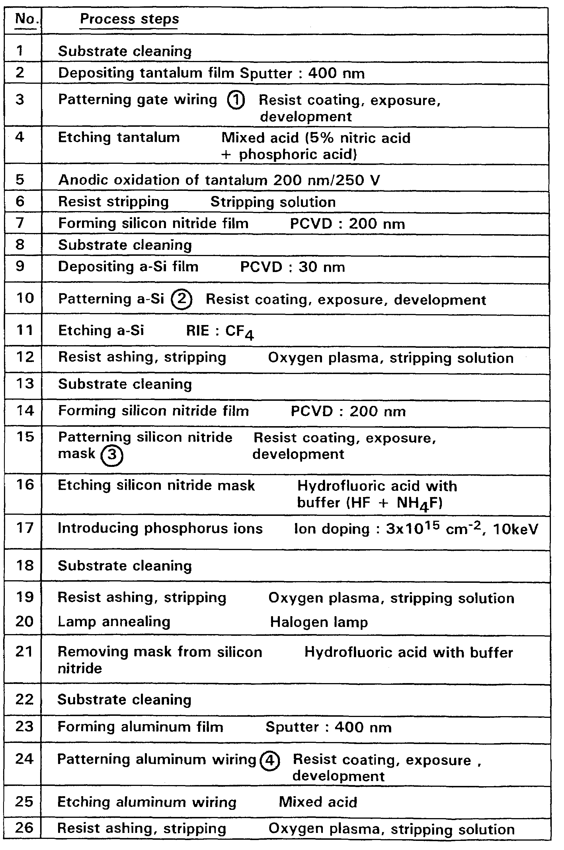
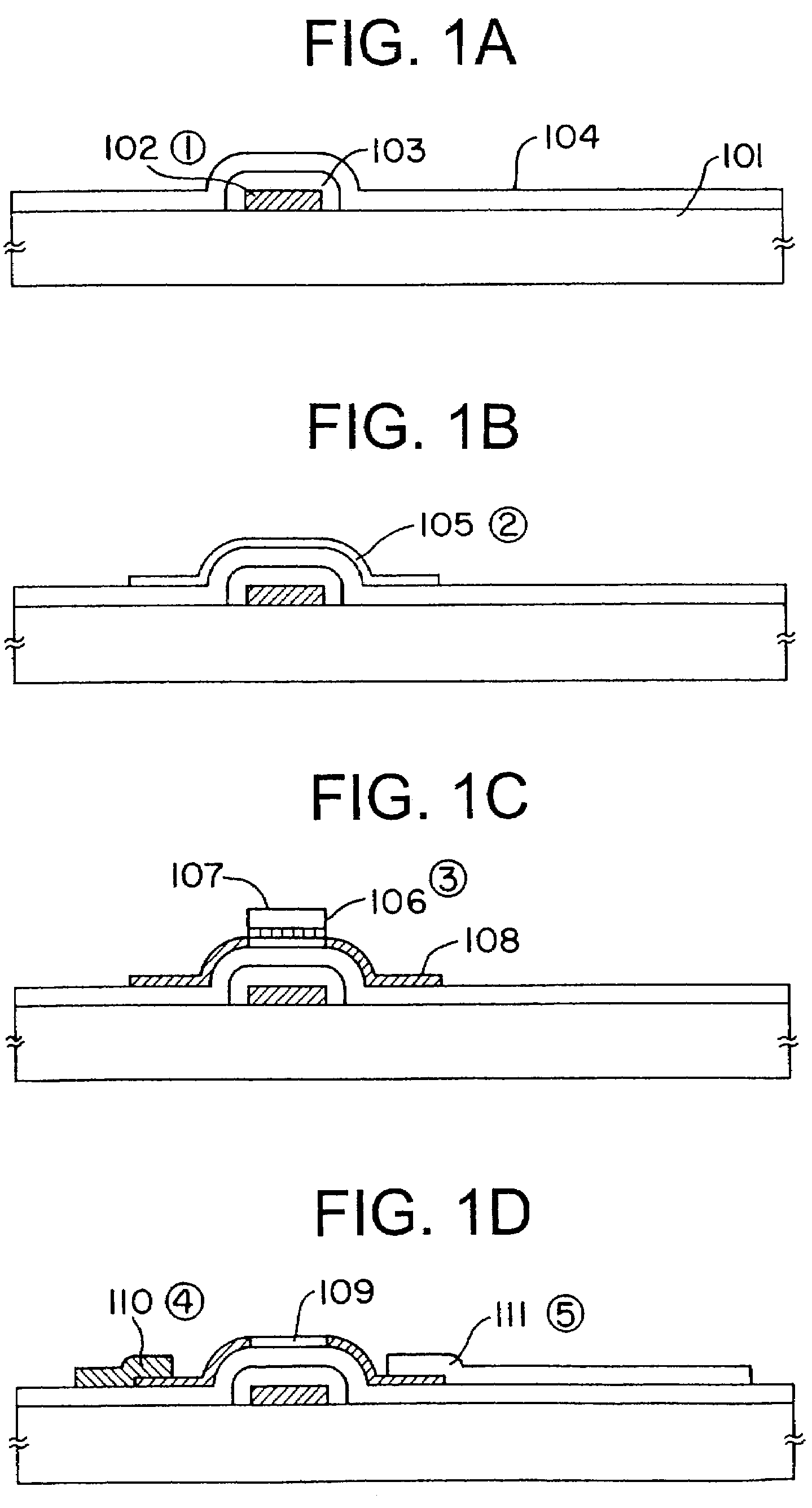
[0052]A TFT was fabricated according to the process steps listed in FIG. 3. FIGS. 1(A) to 1(D) show the schematically drawn step-sequential cross section structures obtained in a process for fabricating a TFT according to an embodiment of the present invention, up to the fabrication of the metal wiring and electrode 110. The step of forming an ITO pixel electrode 111 is not included in the figures. Referring to FIGS. 1(A) to 1(D), the surface of a tantalum gate electrode was coated with about 200 nm thick anodic oxide film in step 5 to improve the insulating properties. The anodic oxide film comprises an oxide of a material constituting the gate electrode. Impurities were doped by means of ion doping. Four masks in total were used in the entire process comprising 26 steps.

[0053]In FIGS. 3 to 6 hereinafter, “sputter”, “PCVD”, and “RIE” refer to a film deposition process using sputtering, a plasma CVD process, and a reactive ion etching process, respectively. The thickness of the depo...

example 2

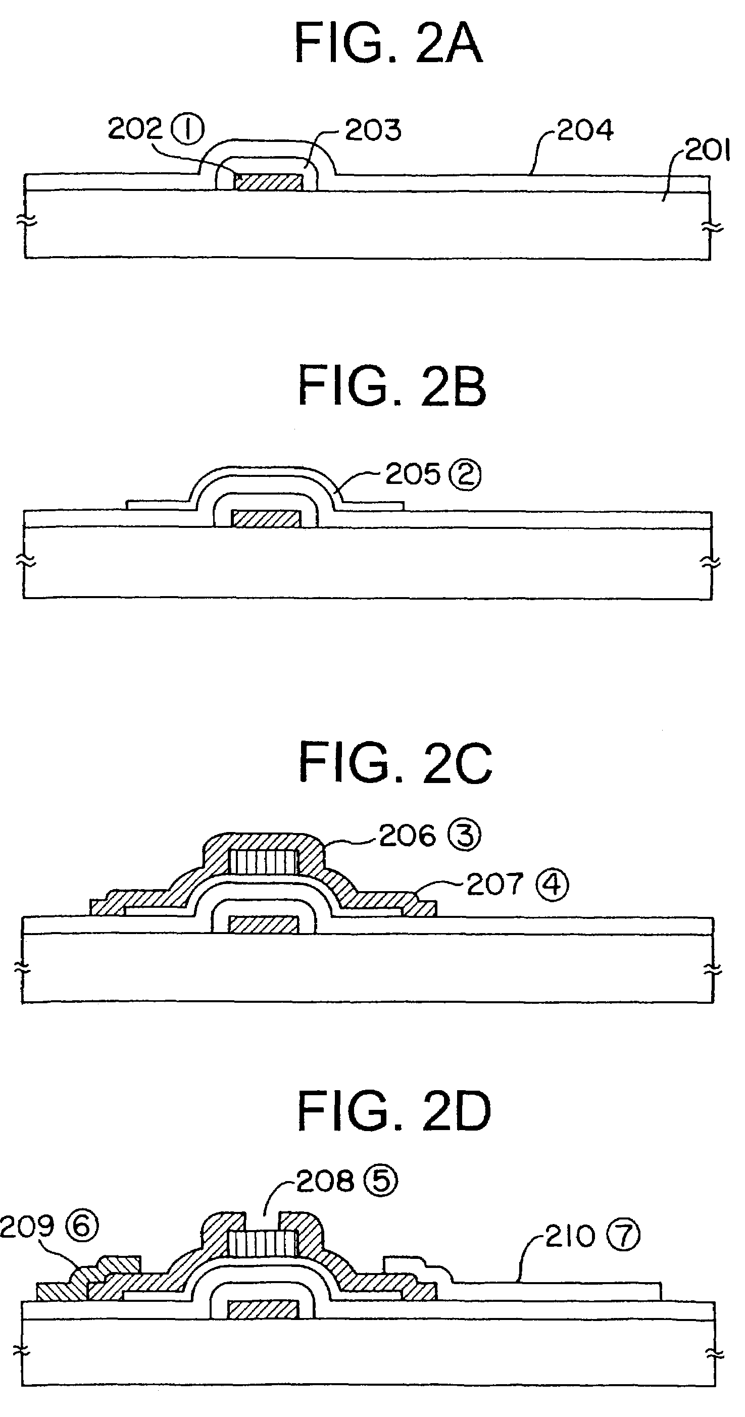
[0065]A TFT was fabricated according to the process steps listed in FIG. 4. The process steps of the present example are essentially the same as those illustrated in FIGS. 1(A) to 1(D) except that the technique of light exposure from the back is used in the present case. Similar to the case in Example 1, FIG. 4 shows the steps up to the fabrication of the metal wiring and electrode 110. Referring to FIGS. 1(A) to 1(D), the surface of a tantalum gate electrode was coated with about 200 nm thick anodic oxide film in step 5 to improve the insulating properties. The silicon nitride mask was formed by the technique of light exposure from the back. Impurities were introduced by means of ion doping. The number of masks in total was reduced to three by employing the back side light exposure technique. Thus, the process comprises 26 steps.

[0066]A corresponding prior art process is illustrated in the process steps in FIG. 6. Three masks in total were used in the process, and the entire proces...


PUM


Abstract

A thin film transistor of reversed stagger type having improved characteristics and yet obtained by a simple process, which is fabricated by selectively doping the semiconductor region on the gate dielectric to form the source, drain, and channel forming regions by using ion implantation, ion doping, or doping a plasma of ions; and then effecting rapid thermal annealing by irradiating a ultraviolet radiation, a visible light, or a near-infrared radiation for a short period of time. The source, drain, and channel forming regions are formed substantially within a single plane.

Description

[0001]Divisional of prior application Ser. No. 08 / 942,440 filed Oct. 1, 1997 now U.S. Pat. No. 6,500,703 issued Dec. 31, 2002, which is a continuation of U.S. Ser. No. 08 / 620,245 filed Mar. 22, 1996 now abandoned, which is a divisional of U.S. Ser. No. 08 / 286,290 filed Aug. 5, 1994 now U.S. Pat. No. 5,530,265 issued Jun. 25, 1996.BACKGROUND OF THE INVENTION[0002]1. Field of the Invention[0003]The present invention relates to an MIS (Metal-Insulator-Semiconductor) device, and particularly, to an MIS transistor. Specifically, the present invention relates to a thin film MIS-type semiconductor device formed on an insulating substrate, and more specifically, to a thin film transistor (TFT). In particular, the present invention relates to a MIS-type semiconductor device of a so-called reversed stagger type comprising a channel forming region on the upper side of a gate electrode. The present invention relates to a semiconductor integrated circuit formed on an insulating substrate, for ex...

Claims


Application Information

Patent Timeline
Patent Type & Authority Patents(United States)
IPC IPC(8): H01L21/84H01L29/40H01L21/26H01L21/265H01L21/336H01L29/78H01L29/786
CPCH01L29/66765H01L29/78669H01L29/78675H01L21/18H01L29/786
Inventor TAKEMURA, YASUHIKO
Owner SEMICON ENERGY LAB CO LTD
Why Eureka
Try Eureka