Photo-field effect transistor and integrated photodetector using the same

a photodetector and photofield effect technology, applied in the direction of diodes, semiconductor devices, electrical apparatus, etc., can solve the problems of not being able to meet the extensive demands of eb-ccd cameras, the detection limit of pin photodiodes is much inferior to a silicon ccd, and it is difficult to combine ccd with an electron multiplying plate requiring an accelerated voltage of 1 kv

Inactive Publication Date: 2010-07-20
NAT INST OF ADVANCED IND SCI & TECH
View PDF21 Cites 15 Cited by
  • Summary
  • Abstract
  • Description
  • Claims
  • Application Information

AI Technical Summary

Benefits of technology

[0042]The present invention has been accomplished in view of the conventional state of affairs. An object thereof is to provide a photo-FET that is not a silicon-based photodetector as disclosed in Documents 2 and 3. Further, an object is to provide a compound semiconductor-based photodetector that is advantageous for expanding a wavelength range, that can eliminate or alleviate the drawbacks in the background art, that can acquire sufficiently high optical sensitivity even with a device dimension readily producible with an ordinary photolithography machine having resolution of approximately 0.5 μm at most, and that can infallibly suppress a leakage current with a two-dimensional or three-dimensional highly reproducible device structure.
[0045]With the above configuration, the dark current (leakage current) in the dark can be suppressed to a great extent compared with the background FETs to enable the provision of a photo-FET that is relatively easier to fabricate and capable of detecting the leakage current efficiently with illumination.
[0050]As still another devised configuration, the channel layer may be formed with plural blind holes arranged at intervals to at least pass through the channel layer when being seen in the cross-sectional direction, and the parts of the channel layer between the adjacent blind holes are allowed to serve as a current-restricted region via which a current can only pass through the channel layer. With this configuration, the effective sensitivity can be enhanced further. In this configuration, it is better that the front-side depletion layer formation layer also covers the side surface of the layer structure that is exposed to the inner wall surfaces of the blind holes.
[0051]As a further embodiment that can structurally prevent a leakage current, a structure can be adopted in which one of the source and drain electrodes is surrounded by the channel layer, whereas the other electrode surrounds the channel layer, when being seen from a plan view.
[0054]While the plural photo-FETs are generally arranged in line-column (two-dimensional matrix arrangement), the present invention can also be applied to the formation of the FET of the same epitaxial layer structure not for photodetection, but for readout in every one line. This makes the formulation of a smart-pixel hybrid integrated circuit easier, which results in great promotion of the development of a small camera with a lock-in detection module having the integrated circuit, a highly sensitive small spectrophotometer, and an optical heterodyne microscope.

Problems solved by technology

In the case of the PMT and avalanche photodiode, however, there are intrinsic problems to establish a detector array, since a highly accelerated voltage is required for accelerating and multiplying electrons generated by light in a vacuum or solid substance, and since there are considerable variations in the multiplication characteristics.
Also in the EB-CCD camera, since an induced electrostatic discharge damages a micro CCD at several volts, it is actually difficult to combine the CCD with an electron multiplying plate requiring an accelerated voltage of 1 KV.
Therefore, the EB-CCD camera as a product is too expensive to reach a level that satisfies extensive demands.
While a PIN photodiode using a compound semiconductor is simple in structure and relatively easy to establish integration, however, detection limit of the PIN photodiode is much inferior to a silicon CCD.
Further, the PIN photodiode is low in sensitivity and is greatly affected by a readout noise from an external amplifier, and has no charge storage mechanism, unlike the silicon CCD.
Another serious problem posed by a background photodetector is that a sensitive wavelength region is limited.
Though an image pickup device has been developed in various aspects within a visible region, the image pickup device has insufficient sensitivity at an ultraviolet region in the wavelength of 150 nm to 300 nm or at an infrared region in the wavelength longer than 1 μm.
The image pickup device has been required to dispose a plurality of photodetectors having different sensitive characteristics to cope with a wavelength region over a wide range, resulting in a complicated optical system.
However, the photogenerated carriers are dissipated without any countermeasures because the respective contact parts of the source and drain have to be deservingly deprived of silicon oxide film for a gate insulator.
The device isolation process of the VMIS is rather difficult since it is a bipolar device.
Thus, the device fabrication process becomes complicated as compared to an ordinary CMOS image sensor.
However, since the light-receiving device per se used in an FPA has no addressing function, realization of an image pickup device requires complicated manufacturing operations such as a wafer thinning process of a two-dimensional compound semiconductor PIN photodetector array and bonding it to a two-dimensional silicon-charge amplifier array.
Furthermore, the FPA has not yet solved the problem of a large influence of a readout noise by an external amplifier since it is required to amplify a minute current induced by photo-generated electron-hole pairs corresponding at most to the number of photons in the incident light, similarly to the case of a discrete PIN photodetector.
This device, however, has some drawbacks.
Since the InGaAs channel layer that serves as a light-absorbing layer is thin, the absorbing efficiency for the long-wavelength light is not good and an improvement such as waveguide coupling is necessary.
Furthermore, since a barrier layer of InAlAs reacts with oxygen or moisture in the atmosphere, the device poses a problem from the standpoint of reliability.
Another problem is that the threshold value is apt to be instable since impurities in the InAlAs are moved easily.
While Al-free InP is advantageous as a gate material from the viewpoint of reliability, some difficulties remain: a Schottky junction is difficult to form; a leakage current is induced from the surface and from the interface between the substrate and the epitaxial layer.
Concerned about a photodetector based on a compound semiconductor-based FET structure, excluding a silicon-based one, it is still impossible to obtain a photo-FET having a sufficiently satisfactory optical sensitivity even when the technique disclosed in Document 6 is used along its gist to fabricate a device, which is considered as being excellent in the background art documents.
Even when the trench-digging technique, as disclosed in Document 7, has been incorporated therein, this cannot be effective according to the experiences of the present inventors because the formation of a dielectric insulation film induces leakage of a current through the surface of the trench.
It is, as a matter of course, undesirable to require such high accuracy for the device fabrication, because of the large number of steps required and their complexity.
Since satisfactory optical sensitivity has not yet been obtained, the background art techniques have not yet reached a level that can sufficiently be advocated in future without any modification.

Method used


Image

  • Photo-field effect transistor and integrated photodetector using the same
  • Photo-field effect transistor and integrated photodetector using the same
  • Photo-field effect transistor and integrated photodetector using the same

Examples


Embodiment Construction

[0077]The present invention will be described in detail with reference to the accompanying drawings.

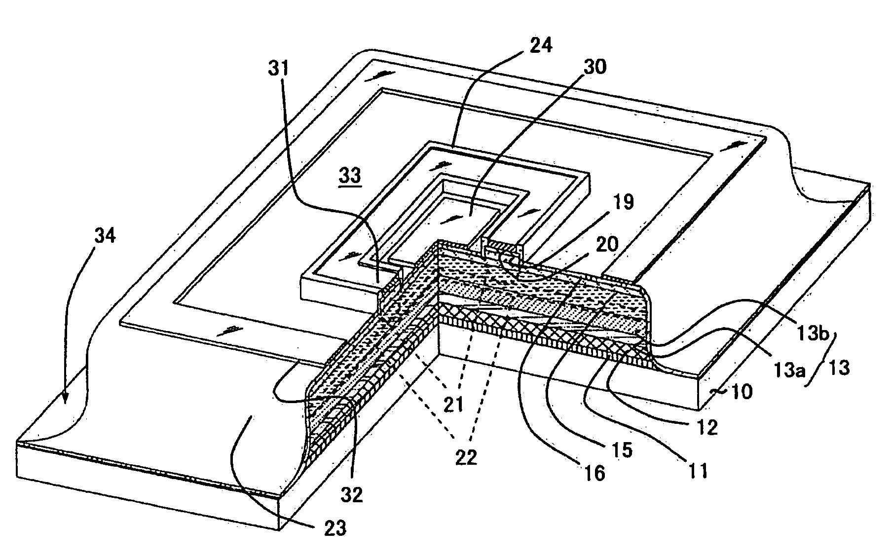
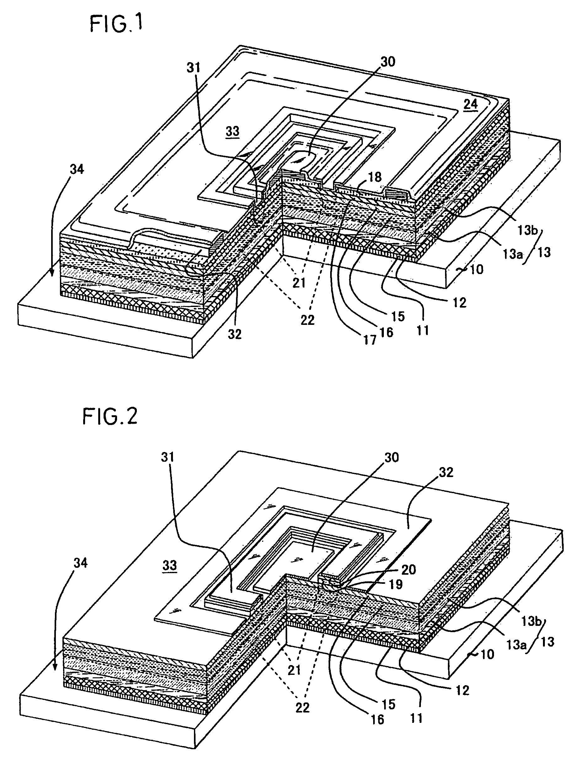
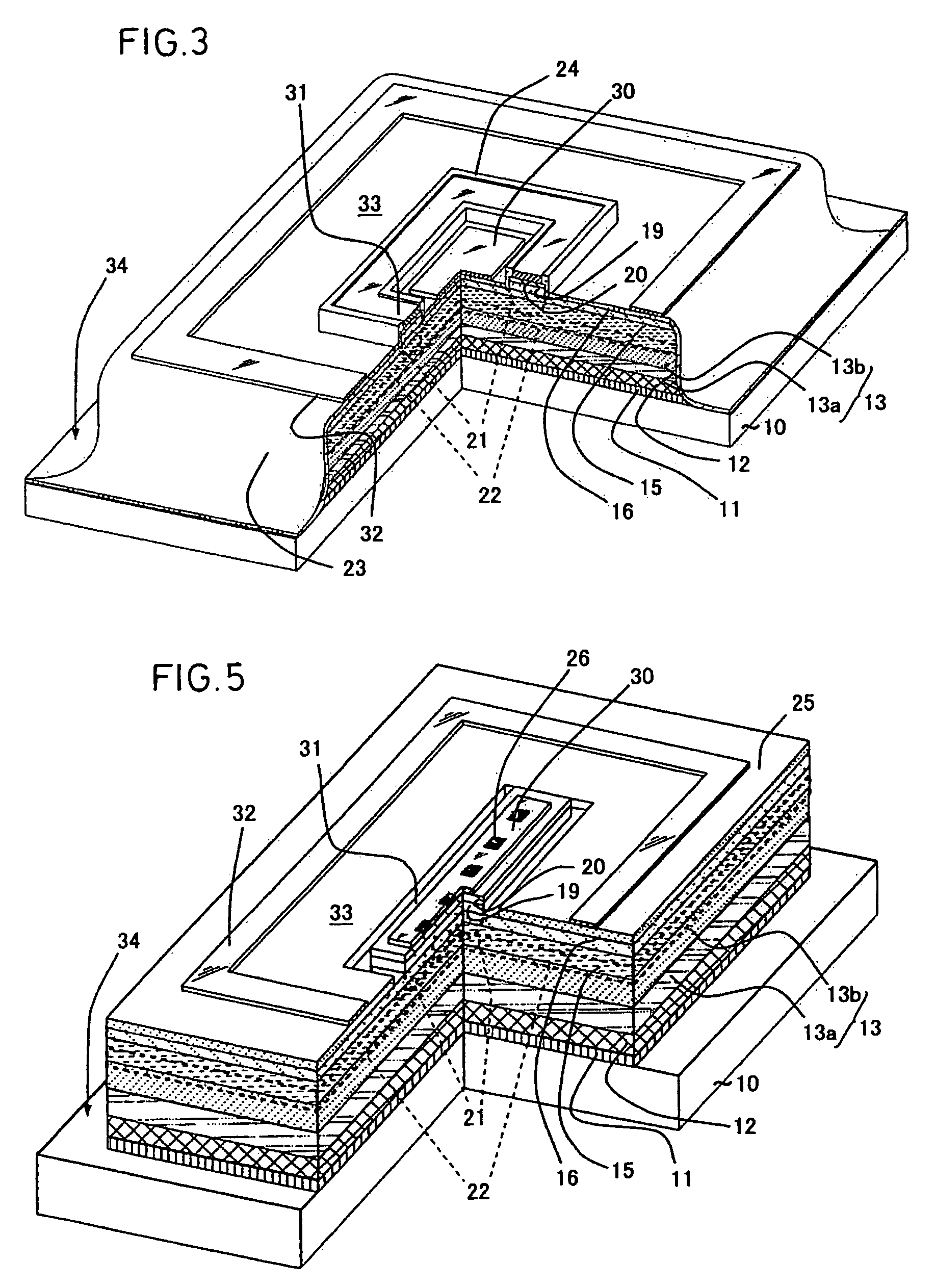
[0078]FIG. 1 shows a preferred embodiment of a photo-FET having a relatively fundamental structure, which has been fabricated according to the present invention.

[0079]Generally, in long wavelength semiconductor materials prepared with the MOCVD, an InGaAs—InP-based material used in the near-infrared region of up to a wavelength of 2.5 μm exhibits an n-type background carrier concentration of around 2×10¹⁴ to 2×1015 cm−3 due to the influence of residual impurities, and an InSb-based or InAsSb-based material used in the infrared region of up to a wavelength of 6 μm exhibits a background carrier concentration of around 1×1016 cm−3. On the other hand, to increase the photo-absorption coefficient, a photo-detector is required to have a light-absorbing layer (photosensitive layer) having a thickness of at least 1 to 2 μm. For this reason, it is necessary to deplete a channel beforehand whic...


PUM


Abstract

A photo-FET based on a compound semiconductor including a channel layer formed on a substrate constituting a current path between source and drain electrodes, serving as part of a photodiode and a photosensitive region. A back-gate layer that serving as a substrate-side depletion layer formation layer is disposed between the substrate and the channel layer, and applies to the channel layer a back-gate bias by photogenerated carriers upon illumination. A barrier layer is disposed on the front side of the channel layer that causes one of the photogenerated carriers to run through the channel layer and other of the photogenerated carriers to sojourn or be blocked off. A front-side depletion layer formation layer is disposed on the front side of the channel layer brings the front-side depletion layer into contact with the substrate-side depletion layer without illumination to close the current path in the channel layer, bringing the photo-FET to an off-state.

Description

CROSS-REFERENCE TO PRIORITY DATA[0001]The present application is a continuation of Application PCT / JP 2007 / 052913 filed on Feb. 13, 2007, and also claims priority to JP 2006-035927 filed on Feb. 14, 2006, the entire contents of each of which are herein incorporated by reference.BACKGROUND OF THE INVENTION[0002]1. Field of the Invention[0003]The present invention relates to an improvement in a photo-field effect transistor (hereinafter referred to also as a “photo-FET”) in which a photodiode and a field-effect transistor (hereinafter referred to also as a “FET”) are integrated monolithically.[0004]2. Discussion of the Background[0005]A photodetector in a near-infrared region, particularly a photodetector array in which plural photodetectors are arranged one- or two-dimensionally, has been in high demand as an infrared photodetector for spectroscopic systems or an infrared camera in a variety of applications in the fields of medicine, disaster prevention and industrial inspection. For...

Claims


Application Information

Patent Timeline
Patent Type & Authority Patents(United States)
IPC IPC(8): H01L29/80
CPCH01L27/14603H01L31/10H01L27/14643H01L29/80H01L29/808
Inventor OGURA, MUTSUO
Owner NAT INST OF ADVANCED IND SCI & TECH
Why Eureka
Try Eureka