Method for preparing silicon hollow nano-cone array

A nanocone and cone array technology, which is applied in nanostructure manufacturing, nanotechnology, nanotechnology, etc., can solve the problems of time-consuming, low efficiency, and difficulty in realizing the construction of silicon nanocone arrays, etc.

Inactive Publication Date: 2009-08-05
JILIN UNIV
View PDF0 Cites 31 Cited by
  • Summary
  • Abstract
  • Description
  • Claims
  • Application Information

AI Technical Summary

Problems solved by technology

The first two methods are time-consuming, difficult to achieve controllable cycle spacing, and difficult to realize the construction of large-area arrays
Electron beam (E-Beam) etching and focused ion beam (FIB) etching can accurately control parameters such as the period and bottom diameter of the silicon nanocone array, but the instruments used are ex

Method used


Image

  • Method for preparing silicon hollow nano-cone array
  • Method for preparing silicon hollow nano-cone array
  • Method for preparing silicon hollow nano-cone array

Examples


Embodiment 1

[0040] 1. Preparation method of polystyrene microspheres:

[0041]Under the protection of nitrogen, using 100 ml of absolute ethanol and 40 ml of deionized water as the dispersion medium, add 10.5 ml of styrene, 0.2222 g of potassium persulfate, and 0.2445 g of sodium dodecyl sulfonate to the machine In the reactor of the stirrer and reflux condenser, the mechanical stirring speed is 300 rpm. The dispersion polymerization reaction was carried out in a water bath at 70°C. After 10 hours of reaction, an emulsion of stable milky white monodisperse polystyrene microspheres was obtained. The diameter of the microspheres was 792 nm.

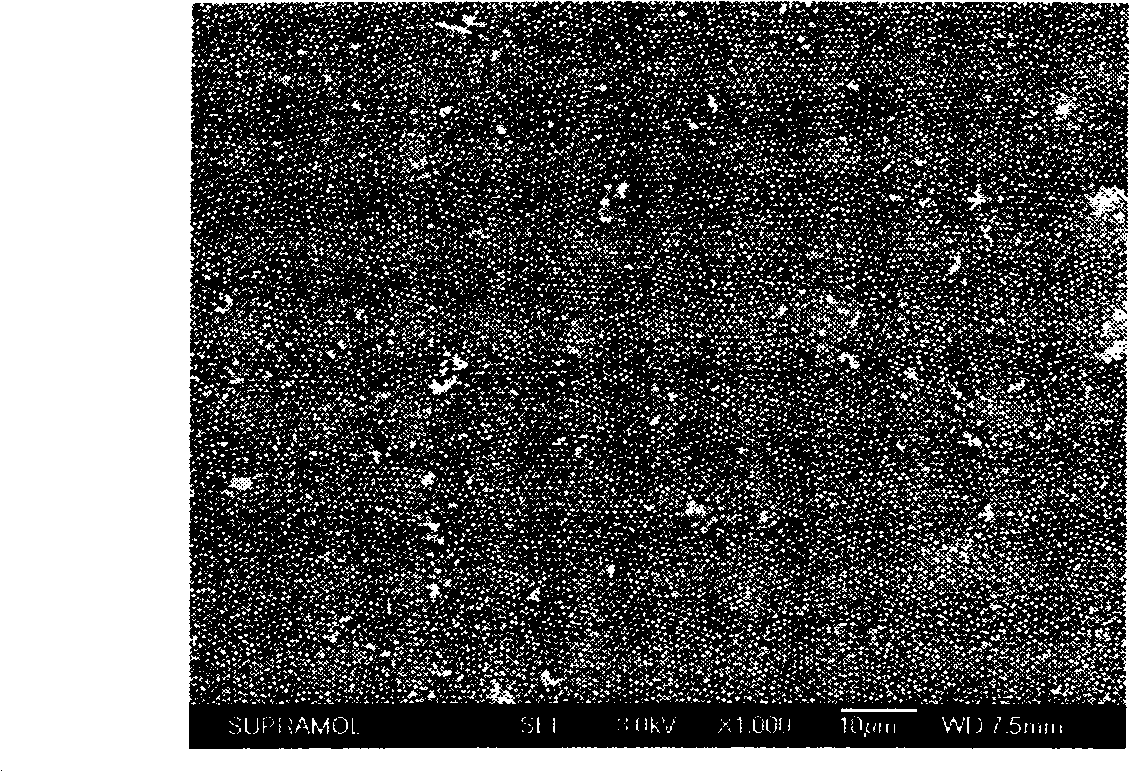
[0042] 2. Preparation of polystyrene monolayer colloidal crystals:

[0043] The prepared polystyrene microspheres were washed by centrifugation, and then dispersed with a mixture solution of absolute ethanol and deionized water with a volume ratio of 1.5:1 to obtain monodisperse polystyrene microspheres with a solid content of 0.5% (mass fraction) Emulsion...

Embodiment 2

[0049] 1. The preparation method of polystyrene microspheres and the preparation method of polystyrene monolayer colloidal crystals are shown in Example 1.

[0050] 2. Preparation of hollow silicon nanopillar array:

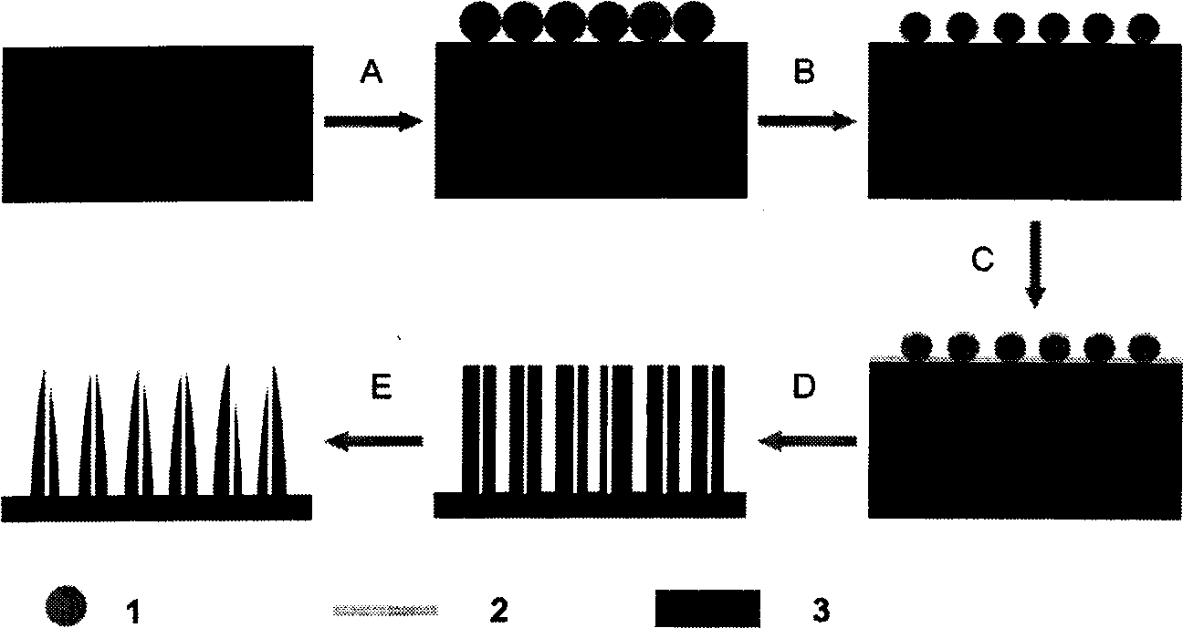
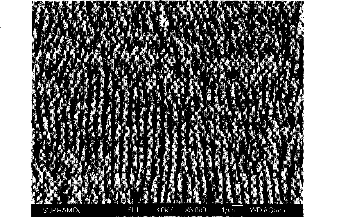
[0051] The preparation method of the non-closely packed colloidal crystals is shown in Example 1, and then a 45nm thick silver film is deposited on the substrate with a vacuum evaporation apparatus; then the sample is immersed in a mixed solution of hydrofluoric acid and hydrogen peroxide (hydrofluoric acid concentration is 4.6 mol / L, the concentration of hydrogen peroxide is 0.44mol / L) for 12 minutes, followed by removing the silver film with aqua regia and removing the polystyrene microspheres with chloroform; obtaining a hollow silicon nanopillar array.

[0052] 3. Construction of hollow silicon nanocone array:

[0053] Perform fluorine reactive ion etching on the obtained hollow silicon nanopillar array, the etching power is RF100W, ICP500W, the cavity pressure ...

Embodiment 3

[0055] 1. The preparation method of polystyrene microspheres and the preparation method of polystyrene monolayer colloidal crystals are shown in Example 1.

[0056] 2. Preparation of hollow silicon nanopillar array:

[0057] The preparation method of non-closely packed colloidal crystals is shown in Example 1, and then a 40nm thick silver film is deposited on the substrate with a vacuum evaporation apparatus; then the sample is immersed in a mixed solution of hydrofluoric acid and hydrogen peroxide (hydrofluoric acid concentration is 4.6 mol / L, the concentration of hydrogen peroxide is 0.44mol / L) for 6 minutes, followed by removing the silver film with aqua regia and removing the polystyrene microspheres with chloroform; obtaining a hollow silicon nanopillar array.

[0058] 3. Construction of hollow silicon nanocone array:

[0059] Perform fluorine reactive ion etching on the obtained hollow silicon nanopillar array, the etching power is RF100W, ICP500W, the cavity pressure is 5m...


PUM

PropertyMeasurementUnit
Sizeaaaaaaaaaa
Diameteraaaaaaaaaa
Heightaaaaaaaaaa

Abstract

The invention relates to a method for preparing a hollow silicon nano conical array, in particular to a method for preparing the hollow silicon nano conical array with large area, uniform bottom diameter length, controllable spacing, controllable period and orderly arrangement. The method comprises the following four steps: washing and surface hydrophilization treatment of a monocrystalline silicon piece, preparation of polystyrene monolayer colloidal crystals, preparation of a hollow silicon nano column array, and construction of a hollow silicon nano conical array. The hollow silicon nano conical array obtained by the method has the advantages of large area, uniform bottom diameter length, controllable spacing, controllable period and orderly arrangement, has extremely superior broad-band dereflection performance, and effectively reduces the surface reflection loss from deep ultraviolet band to medium infrared band (250 nanometers to 15 mu m). The method is simple and controllable, and has wide application prospect on construction of photoelectric devices with low cost and large area and deflection surfaces.

Description

Technical field [0001] The invention relates to a preparation method of a silicon hollow nanocone array, in particular to a preparation method of a silicon hollow nanocone array with a large area, uniform bottom diameter, controllable spacing, controllable period, and orderly arrangement. Background technique [0002] Silicon is the most important material in the semiconductor industry today. Due to the asymmetry of the silicon nanocone shape and the pointed tip, the array has a wide range of applications, such as anti-reflection coatings, high-efficiency field emission devices, and high-sensitivity sensors , Self-cleaning surface, etc. [0003] There are roughly three existing methods for preparing silicon nanocone arrays: chemical vapor deposition methods, laser ablation methods, and etching methods. The first two methods are time-consuming, difficult to achieve controllable periodic spacing, and difficult to achieve large-area array construction. Electron beam (E-Beam) etching...

Claims


Application Information

Patent Timeline
IPC IPC(8): B82B3/00
Inventor 杨柏李云峰张俊虎朱守俊贾菲
Owner JILIN UNIV
Why Eureka
Try Eureka