Method for preparing gold nanocrystals with high density at room temperature and applications thereof

A gold nano, high-density technology, applied in the direction of nanotechnology, nanotechnology, nanostructure manufacturing, etc., can solve the problems of increasing device thermal stress, increasing memory energy consumption and cost, and unfavorable processing of nanodevices, so as to avoid thermal stress Produces, maintains stable, fully isolated effects

Inactive Publication Date: 2009-11-11
FUDAN UNIV
View PDF1 Cites 2 Cited by
  • Summary
  • Abstract
  • Description
  • Claims
  • Application Information

AI Technical Summary

Problems solved by technology

[0006] The above method uses high temperature heat treatment, which not only increases the energy consumption and cost in the memory manufa...

Method used


Image

  • Method for preparing gold nanocrystals with high density at room temperature and applications thereof
  • Method for preparing gold nanocrystals with high density at room temperature and applications thereof
  • Method for preparing gold nanocrystals with high density at room temperature and applications thereof

Examples


Embodiment 1

[0036] A method for preparing high-density gold nanocrystals at room temperature, comprising the steps of:

[0037] A, the preparation of gold sol:

[0038] The first step: add 1 milliliter of chloroauric acid water with a mass volume concentration of 1 to 3% into a flask filled with 100 milliliters of ultrapure water, and stir vigorously for 1 to 2 minutes;

[0039] The second step: add 1 ml of sodium citrate aqueous solution with a mass volume concentration of 1 to 3% dropwise in the mixed solution of the first step within 1 minute, and mix for 1 to 2 minutes;

[0040] Step 3: Add 1 milliliter of sodium borohydride solution (dissolved in a 1% sodium citrate aqueous solution) with a mass volume concentration of 0.065 to 0.085% in the above mixed solution, and continue stirring until the solution becomes Wine red color, gold sol configuration is completed, and the system temperature is maintained at room temperature throughout the preparation process.

[0041] B. Preparation...

Embodiment 2

[0052] A method for preparing high-density gold nanocrystals at room temperature, comprising the steps of:

[0053] A, the preparation of gold sol: with embodiment 1

[0054] B. Preparation of high-density gold nanocrystals:

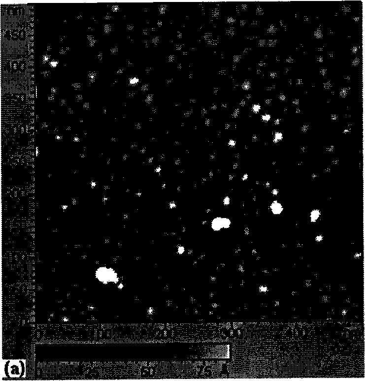
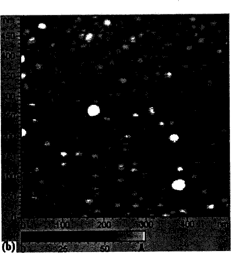
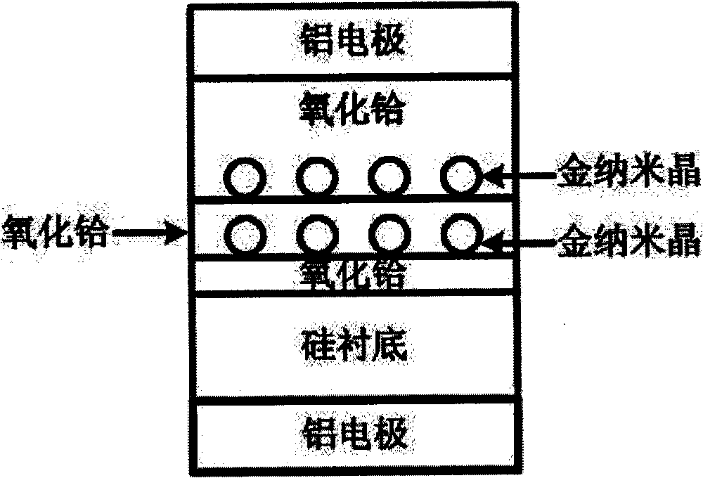
[0055] Step 1: In the atomic layer deposition reaction chamber, after standard cleaning of the p-type silicon wafer, atomic layer deposition of HfO with a thickness of 5 to 7 nanometers on the surface of the p-type silicon wafer 2 thin films, in which atomic layer deposited HfO 2 The reaction precursor of the film is tetrakis-(ethylmethylamino) hafnium (TEMAH) and water, and the deposition temperature is controlled at 280-320°C;

[0056] Step 2: Cover with HfO 2 The p-type silicon chip of the film is soaked in an aqueous solution of 5% aminopropyltrimethoxysilane (APTMS) in mass concentration, taken out after two hours, rinsed with a large amount of ultrapure water, and treated with ultrasound several times;

[0057] Step 3: Put the p-type silicon ch...


PUM

PropertyMeasurementUnit
Thicknessaaaaaaaaaa
Sizeaaaaaaaaaa
Thicknessaaaaaaaaaa

Abstract

The invention discloses a method for preparing gold nanocrystals with high density at room temperature, comprising the following steps of: firstly using an atomic layer to deposit to form an Al2O3 thin film or an HfO2 thin film on a substrate; soaking the Al2O3 thin film or the HfO2 thin film in aminopropyl trimethoxy silane aqueous solution with the mass concentration being of 3-8 percent for 1.5-3 hours; putting the Al2O3 thin film or the HfO2 thin film into aerosol, and soaking for 3-8 hours; and self-assembling the gold nanocrystals on the surface of the Al2O3 thin film or the HfO2 thin film. Furthermore, two metal electrodes which can be prepared into capacitance elements are formed by sputtering or electron beam evaporation on the surfaces of the backside and topside of the substrate respectively. The method has the advantages that the performance at room temperature avoids that the traditional high temperature treatment technology easily causes the gold nanocrystals formed more previously to suffer high temperature heat treatment for multiple times, thus ensuring the stable property of the gold nanocrystals which grow by self assembly; the obtained nanocrystal array has good uniformity; and the atomic layer deposition method realizes that Al2O3 and HfO2 can grow at the temperature lower than 350 DEG C, and the thickness of the thin film can be controlled precisely.

Description

technical field [0001] The invention belongs to the technical field of semiconductor memory manufacturing, in particular to a method and product for preparing high-density gold nanocrystals at room temperature. technical background [0002] With the widespread application of polysilicon floating gate memory in the fields of communication, consumption, and computer, it has become a memory chip product occupying a certain market share. However, the scaling-down requirement of the semiconductor industry poses a great challenge to the quality of the nanometer-thick tunnel oxide layer. [0003] Nanocrystalline memory solves the dilemma of tunnel oxide layer thinning and data retention degradation that traditional polysilicon floating gate memory encounters when its size is further reduced. See literature [1] A.Thean, J.P.Leburton, "Flash memory: towardssingle-electronics", IEEE Potentials, 2002, 21 (Oct / Nov), pp.35-41. Its advantage is that the charge is stored in discrete nanoc...

Claims


Application Information

Patent Timeline
IPC IPC(8): B82B3/00H01L21/02H01L21/8247H01L27/11568
Inventor 黄玥丁士进
Owner FUDAN UNIV
Why Eureka
Try Eureka