
Preparation method for photonic crystal structure film electrode of dye solar cell

A technology for solar cells and photonic crystals, applied in capacitor electrodes, photosensitive devices, electric solid devices, etc., can solve the problems of high cost, wide application limitation, and inability to mass-produce, and achieves light weight, simplified process, high short-circuit current and the effect of the fill factor

Inactive Publication Date: 2010-06-23
SHANGHAI JIAO TONG UNIV
View PDF7 Cites 20 Cited by
  • Summary
  • Abstract
  • Description
  • Claims
  • Application Information

AI Technical Summary

Problems solved by technology

However, in order to manufacture electrode materials with highly periodic photonic crystal structures, laser etching technology combined with dry etching technology can only be used to manufacture samples individually in the laboratory, and the cost is high and cannot be mass-produced. Broad application is limited

Method used


Image

  • Preparation method for photonic crystal structure film electrode of dye solar cell
  • Preparation method for photonic crystal structure film electrode of dye solar cell
  • Preparation method for photonic crystal structure film electrode of dye solar cell

Examples


Embodiment 1

[0033] (1) FTO conductive glass is cut into 1cm×4cm glass slides, soaked in piranha solution (3:1 H2SO4:30% H2O2) for 24 hours, and then washed with deionized water. 10g monomer styrene, 0.74g methacrylic acid and 0.1g potassium persulfate were mixed into 100ml deionized water, and the temperature was raised to 75°C under nitrogen gas to carry out soap-free emulsion polymerization for about 10 hours.

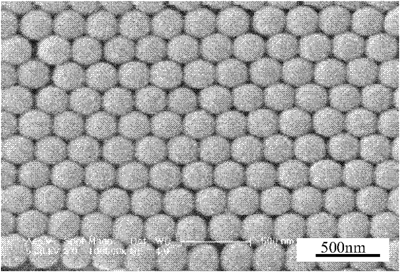
[0034] (2) After 5 centrifugal filtration and purification of the obtained polystyrene colloid, it was diluted with deionized water at a volume ratio of 0.2% to a monodisperse polystyrene bead solution, and poured into a glass vial with a vertical FTO slide; and Place it in a drying oven with a constant temperature of 45°C (±0.5) and a humidity of 90% (±2%) to grow for a week, and a light red smooth film is formed on the surface, which is used as a photonic crystal positive template.

[0035] (3) Dissolve tetra-n-butyl titanate in 100 ml of absolute ethanol at a volume ratio of 5%, a...

Embodiment 2

[0040] (1) Cut the FTO conductive glass into 1cm×4cm glass slides, soak in piranha solution (3:1 H2SO4:30% H2O2) for 24 hours and then rinse with deionized water. 10g monomer styrene, 0.5g methacrylic acid and 0.1g potassium persulfate were mixed into 100ml deionized water, and the temperature was raised to 75°C under nitrogen gas to carry out soap-free emulsion polymerization for about 10 hours.

[0041] (2) After 5 centrifugal filtration and purification of the obtained polystyrene colloid, it was diluted with deionized water at a volume ratio of 0.2% to a monodisperse polystyrene bead solution, and poured into a glass vial with a vertical FTO slide; and Place it in a drying oven with a constant temperature of 45°C (±0.5) and a humidity of 90% (±2%) to grow for a week. A light green smooth film is formed on the surface, which is used as the positive template of the photonic crystal.

[0042] (3) Dissolve tetra-n-butyl titanate in 100 ml of absolute ethanol at a volume ratio of 5%...

Embodiment 3

[0048] (1) FTO conductive glass is cut into 1cm×4cm glass slides, soaked in piranha solution (3:1 H2SO4:30% H2O2) for 24 hours, and then washed with deionized water. 10g monomer styrene, 0.3g methacrylic acid and 0.1g potassium persulfate were mixed into 100ml deionized water, and the temperature was raised to 75°C under nitrogen gas to carry out soap-free emulsion polymerization for about 10 hours.

[0049] (2) After 5 centrifugal filtration and purification of the obtained polystyrene colloid, it was diluted with deionized water at a volume ratio of 0.2% to a monodisperse polystyrene bead solution, and poured into a glass vial with a vertical FTO slide; and Place it in a drying oven with a constant temperature of 45°C (±0.5) and a humidity of 90% (±2%) to grow for a week. A lavender smooth film is formed on the surface, which is used as a positive template for the photonic crystal.

[0050] (3) Dissolve tetra-n-butyl titanate in 100 ml of absolute ethanol at a volume ratio of 5%,...


PUM

PropertyMeasurementUnit
pore sizeaaaaaaaaaa
thicknessaaaaaaaaaa
diameteraaaaaaaaaa

Abstract

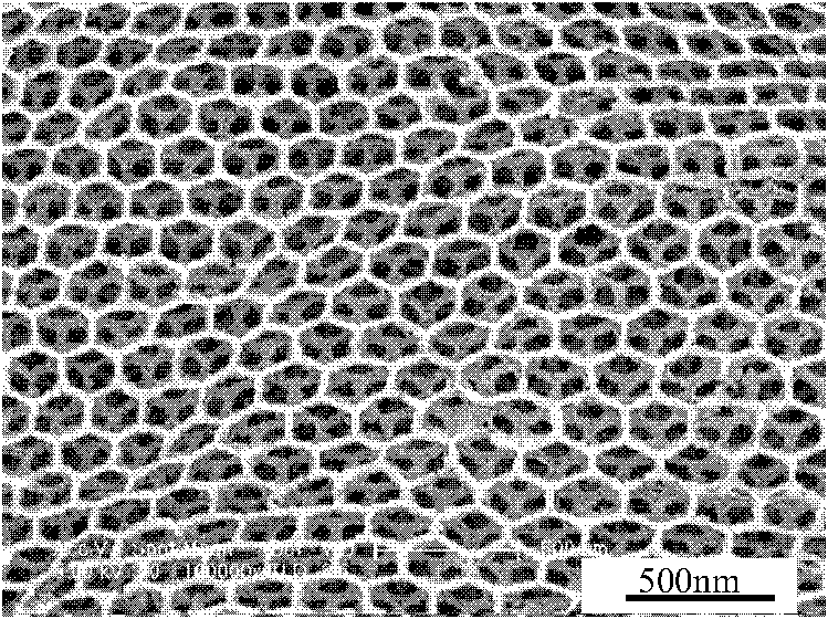
The invention discloses a preparation method for a photonic crystal structure film electrode of a dye solar cell in the technical field of solar cells. A photonic crystal structure positive template structure is introduced into the solar cell and is packaged combined with a pyridine complex dye of ruthenium so as to form the photonic crystal dye solar cell with improved efficiency. A photonic crystal structure positive template is prepared through emulsifier-free emulsion polymerization and a vertical deposition method, and a titanium dioxide photonic crystal reverse template is prepared through a sandwich treatment topology, thereby improving an electrode structure of the traditional dye cell, exceeding the limitation of laboratory photo-etching processing and enhancing the application potential thereof. The prepared photonic crystal structure film electrode takes a three-dimension ordered anatase type titanium dioxide hole arranged by an inverse opal structure as the electrode of the dye solar cell, the hole diameter of film materials thereof ranges from 50nm to 500nm, and the thickness ranges from 0.5 micron to 40 microns, thereby enlarging the specific surface area combined with the dye and having higher short circuit current and filling factors.

Description

Technical field [0001] The invention relates to a preparation method in the technical field of solar cells, in particular to a preparation method of a photonic crystal structure thin film electrode for dye solar cells. Background technique [0002] As one of the protagonists of the third-generation solar energy technology, thin-film solar cells are different from traditional crystalline silicon cells. They have the advantages of low cost, light weight, sufficient raw materials, and ability to work under low light. In addition to CIGS (CuInGaSe), CdTe and amorphous / microcrystalline silicon and other thin film batteries that have begun mass production, Swiss M. The Dye Sensitized Solar Cells (DSSC) developed by the professor's research team is unique with its abundant and cheap raw materials and simple production. It replaces the plate electrode with a porous titanium dioxide electrode, and introduces metal ruthenium (Ru) bipyridine complex dye as a donor that is excited by photon...

Claims


Application Information

Patent Timeline
Patent Type & Authority Applications(China)
IPC IPC(8): H01G9/04H01G9/20H01M14/00H01L51/48
CPCY02E10/50Y02E10/549Y02P70/50
Inventor 胡晓斌邓文歆张荻赵斌元
Owner SHANGHAI JIAO TONG UNIV
Learn More