Selective etching and formation of xenon difluoride

A selective, etching technology, applied in the direction of cleaning methods and appliances, chemical instruments and methods, electrical components, etc., can solve the problem of unacceptable removal of TiN deposition products

Active Publication Date: 2010-09-29
VERSUM MATERIALS US LLC
View PDF8 Cites 7 Cited by
  • Summary
  • Abstract
  • Description
  • Claims
  • Application Information

AI Technical Summary

Problems solved by technology

Many conventional fluorine-based etchants that attack TiN films also attack SiO 2 and SiN surfaces, therefore not acceptable for removal of TiN deposition products from semiconductor deposition chambers and equipment

Method used


Image

  • Selective etching and formation of xenon difluoride
  • Selective etching and formation of xenon difluoride
  • Selective etching and formation of xenon difluoride

Examples


Embodiment 1

[0069] XeF at various temperatures and pressures 2 Effectiveness in etching of deposited materials

[0070] In this example, using XeF 2 As an etchant, measured for TiN, SiO 2 and SiN etch rate. The test samples were coated with TiN, SiO 2 and SiN thin films on silicon wafers. The etch rate is calculated from the change in film thickness between the initial film thickness and the film thickness after timed exposure to etching or processing conditions.

[0071] For etching, a large amount of XeF 2 Gases were introduced from gas cylinders into the reactor chamber via a never-used remote plasma generator. The XeF 2 The pressure of the gas in the reactor chamber was kept constant by shutting off the gas flow from the cylinder once the desired pressure was reached.

[0072] The test specimens were placed on the surface of a pedestal heater used to maintain different substrate temperatures. The results are shown in Table I below.

[0073] Table I

[0074] Use XeF 2 Etch ...

Embodiment 2

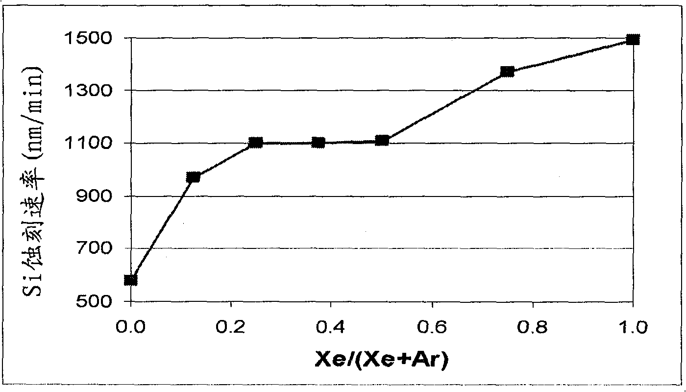
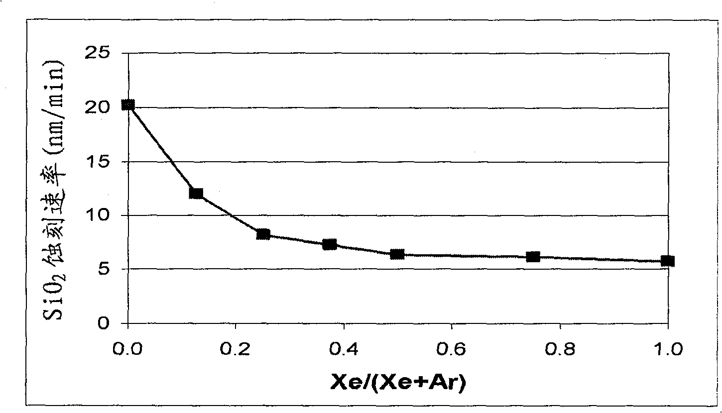
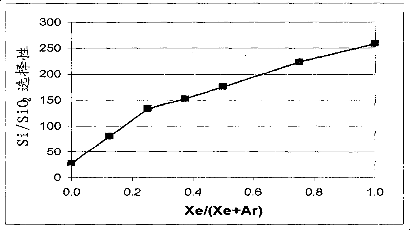
[0079] Silicon vs. SiO 2 selective etching of

[0080] In this example, a MKS Astron remote plasma generator was mounted on top of the reactor chamber. The distance between the outlet of the Astron generator and the sample specimen was approximately six inches. Turn on the remote plasma generator, but turn off the pedestal heater in the reactor chamber. The chamber was kept at room temperature. For Si and SiO using remote plasma 2 The etch rates of both substrates were measured.

[0081] The process gas for the remote plasma is NF 3 , and it is mixed with various amounts of the second gas stream. The second gas stream includes Xe, argon (Ar), or combinations thereof. The total gas flow rate to the reactor chamber was fixed at 400 sccm, and the NF 3 The flow rate was fixed at 80 sccm. While maintaining the total flow rate of the second gas stream at 320 sccm, the ratio of the Xe flow rate to the total flow rate of the second gas stream (Xe / (Ar+Xe)) was at 0 (Ar only as...

Embodiment 3

[0088] Molybdenum (Mo) vs. SiO 2 selective etching of

[0089]A large cylindrical SS etch chamber 2.5 m long and 25 cm in diameter was used to determine the etch rate of another common sacrificial material in MEMS applications: molybdenum (Mo). The remote plasma was generated using a water cooled MKS Astron AX76706 slpm unit. The plasma source was connected to the chamber by a 10 cm long delivery tube with an internal diameter of 4 cm. The sample was placed 2 feet from the load / unload end of the tube.

[0090] At 2.75 Torr, NF 3 At a flow rate of 275 sccm and a Xe or Ar flow rate of 600 sccm, the etch rate of Mo = 1.1 μm / min. SiO 2 The etch rate for NF 3 / Ar gas mixture is 82nm / min, while for NF 3 / Xe mixture at 26 nm / min. Therefore, Xe / NF 3 The selectivity of the mixture is Ar / NF 3 The selectivity of the mixture is at least 3 times. Note that the Mo etch rate is limited by the surface oxide. The etch rate of Mo can be increased to >2.7 microns / minute with surface ...


PUM


Abstract

This invention relates to a process for selective removal of materials, such as: silicon, molybdenum, tungsten, titanium, zirconium, hafnium, vanadium, tantalum, niobium, boron, phosphorus, germanium, arsenic, and mixtures thereof, from silicon dioxide, silicon nitride, nickel, aluminum, TiNi alloy, photoresist, phosphosilicate glass, boron phosphosilicate glass, polyimides, gold, copper, platinum, chromium, aluminum oxide, silicon carbide and mixtures thereof. The process is related to the important applications in the cleaning or etching process for semiconductor deposition chambers and semiconductor tools, devices in a micro electro mechanical system (MEMS), and ion implantation systems. Methods of forming XeF2 by reacting Xe with a fluorine containing chemical are also provided, where the fluorine containing chemical is selected from the group consisting of F2, NF3, C2F6, CF4, C3F8, SF6, a plasma containing F atoms generated from an upstream plasma generator and mixtures thereof.

Description

[0001] Cross References to Related Applications [0002] This application is a continuation-in-part of U.S. Patent Application Serial No. 11 / 285,056, filed November 22, 2005, entitled "SELECTIVE ETCHING OFTITANIUM NITRIDE WITH XENON DIFLUORIDE." technical field [0003] This invention relates to the selective etching and formation of xenon difluoride. Background technique [0004] Various deposition techniques have been developed in the electronics industry in which selected materials are deposited on a target substrate to fabricate electronic components such as semiconductors. One deposition process is chemical vapor deposition (CVD), in which gaseous reactants are introduced into a heated process chamber to obtain a film deposited on a desired substrate. A subtype of CVD is known as plasma enhanced CVD (PECVD), in which a plasma is established in a CVD process chamber. [0005] In general, all deposition methods result in accumulation of film and particulate material on ...

Claims


Application Information

Patent Timeline
Patent Type & Authority Applications(China)
IPC IPC(8): H01L21/00B08B7/00C23F1/12
CPCC23F1/02C23F1/12H01L21/3065
Inventor 吴定军E·J·小卡瓦基A·马利卡朱南A·D·约翰逊
Owner VERSUM MATERIALS US LLC
Why Eureka
Try Eureka