Film system structure for enhancing Terahertz radiation absorption rate and preparation method thereof

A technology of terahertz radiation and film structure, which is applied in the field of film structure and its preparation to enhance the absorption rate of terahertz radiation, can solve the problems of low reflectivity, hinder heat transmission, large thermal resistance, etc., so as to improve the surface body of the film. ratio, the preparation process is simple and reasonable, and the effect of increasing the absorption rate of terahertz radiation

Active Publication Date: 2012-07-04
UNIV OF ELECTRONIC SCI & TECH OF CHINA
View PDF4 Cites 35 Cited by
  • Summary
  • Abstract
  • Description
  • Claims
  • Application Information

AI Technical Summary

Problems solved by technology

Black resins are also less reflective, but are thicker and have greater th

Method used


Image

  • Film system structure for enhancing Terahertz radiation absorption rate and preparation method thereof
  • Film system structure for enhancing Terahertz radiation absorption rate and preparation method thereof
  • Film system structure for enhancing Terahertz radiation absorption rate and preparation method thereof

Examples


Embodiment 1

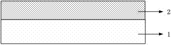
[0038] As shown in Figure 2, a film structure for enhancing the absorption rate of terahertz radiation includes a dielectric thin film and a terahertz absorbing layer, and the structure is deployed on the top layer of the detection unit of the terahertz microarray detector.

[0039] The detection unit of the terahertz microarray detector such as Figure 2-a shown. The array unit is prepared on the silicon wafer with the underlying readout circuit 4, wherein the readout circuit has an interface 5 with the subsequent MEMS device, and then grows a sacrificial layer 6, a supporting layer 7, metal electrodes and leads 8, and a sensitive film 9 etc. and graph them separately. The sacrificial layer material can be silicon oxide film or photosensitive polyimide (PSPI) material; the support layer material is composed of silicon nitride, silicon oxide or multi-layer composite film; the metal electrode is aluminum, titanium, nickel-chromium alloy, etc. ; Sensitive films are vanadium ox...

Embodiment 2

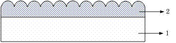
[0045] As shown in Fig. 3, a film structure for enhancing the absorption rate of terahertz radiation includes a dielectric film and a terahertz absorbing layer, and the structure is deployed on the top layer of the pyroelectric terahertz detection unit.

[0046] Pyroelectric terahertz detection unit such as Figure 3-a shown. The completed process is: remove a part of the semiconductor substrate 12 by chemical etching, and then prepare the silicon dioxide dielectric layer 13 , the lower electrode 14 , the lithium tantalate pyroelectric thin film 15 and the upper electrode 16 . Clean the top surface of the detection unit to remove surface contamination, and bake the substrate at 200°C to remove surface moisture and enhance the adhesion of the dielectric film.

[0047] The silicon oxide dielectric thin film 17 is prepared by PECVD frequency mixing growth technology. Two sets of power sources with different frequencies are used to work alternately, among which, the frequency of...

Embodiment 3

[0051] As shown in Figure 4, a film structure for enhancing the absorption rate of terahertz radiation includes a dielectric thin film and a terahertz absorbing layer, and the structure is developed on the top layer of the lithium tantalate crystal sheet sensitive element.

[0052] The preliminary preparation process of lithium tantalate crystal sheet sensitive element is as follows: Figure 4-a~Figure 4-c shown. The preparation process is as follows: the lower electrode 20 is prepared on the lithium tantalate wafer 19, and the lithium tantalate wafer is bonded to the silicon substrate 22 with a BCB polymer material 21, such as Figure 4-a Shown; Lithium tantalate wafer is thinned by grinding and polishing, such as Figure 4-b Shown; Prepare upper electrode 23, as Figure 4-c shown.

[0053] The silicon nitride dielectric thin film 24 is prepared by PECVD frequency mixing growth technology. Two sets of power sources with different frequencies are used to work alternately, ...


PUM

PropertyMeasurementUnit
Thicknessaaaaaaaaaa
Thicknessaaaaaaaaaa

Abstract

The invention discloses a film system structure for enhancing Terahertz radiation absorption rate and a preparation method of the film system structure, wherein the film system structure is located at the top layer of a sensitive unit of a Terahertz detector and comprises a dielectric thin film and a Terahertz absorption layer located on the dielectric thin film; the dielectric thin film is a low-stress silicon nitride or silicon oxide thin film prepared by PECVD (Plasma Enhanced Chemical Vapor Deposition) frequency-mixing technology and etched into a micro nanometer-level rough surface by reactive ions; and the Terahertz absorption layer is prepared on the rough-surface dielectric thin film via a magnetic control sputtering method. As surface-to-volume ratio of the Terahertz absorption layer is increased by the rough surface structure of the dielectric thin film, the Terahertz radiation absorption rate is effectively enhanced; and the preparation process is simple and reasonable, and large-area preparation and integration are easy to carry out, so that the film system structure can be widely applied to the field of various Terahertz detecting and imaging technologies and strong support is provided to the development of high-performance Terahertz detectors.

Description

technical field [0001] The invention relates to the technical field of terahertz detection and imaging, in particular to a film structure for enhancing terahertz radiation absorption rate and a preparation method thereof. Background technique [0002] Terahertz refers to electromagnetic waves with a frequency in the range of 0.1-10THz (1 THz = 1012 Hz), and its corresponding wavelength range is 3mm-30μm, which is between millimeter waves and infrared waves. The development of terahertz science and technology depends on the development of basic disciplines such as physics, chemistry, materials science, optics, and microelectronics, and it also promotes these basic disciplines. It is recognized by the international scientific and technological community that terahertz is an important cross-cutting frontier field. For a long time, due to the lack of effective THz generation and detection methods, people's understanding of the properties of electromagnetic radiation in this ban...

Claims


Application Information

Patent Timeline
IPC IPC(8): B32B9/04B32B15/00G01J5/02
Inventor 王军蒋亚东苟君吴志明黎威志
Owner UNIV OF ELECTRONIC SCI & TECH OF CHINA
Why Eureka
Try Eureka