Flexible base material and preparation method thereof
A flexible substrate, insulating substrate technology, applied in circuit substrate materials, printed circuit manufacturing, printed circuit components, etc., can solve the problems of reduced peel strength, easy detachment of surface chemical groups, and large environmental pollution, achieving Improve peel strength, simple preparation process and good etching performance
- Summary
- Abstract
- Description
- Claims
- Application Information
AI Technical Summary
Problems solved by technology
Method used
Image
Examples
preparation example Construction
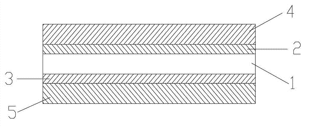
[0026] The invention provides a method for preparing a flexible base material, comprising the following steps: A) spraying a metal oxidizing solution and a reducing solution onto the surface layer of an insulating base material at the same time to obtain an insulating base material covered with an intermediate layer. The surface layer contains nanoparticles with a microporous structure, and the thickness of the surface layer is preferably 1-3 μm, more preferably 1-2 μm; B) Put the insulating substrate covered with the intermediate layer into the electroplating solution, and perform electroplating Anti-oxidation treatment yields a flexible substrate. The electroplating solution is an electroplating solution well known to those skilled in the art.
[0027] Wherein, the coverage rate of the nanoparticles on the surface layer is 10%~100%, preferably 35%~80%, the particle size of the nanoparticles is less than 500nm, preferably 100~300nm, and the nanoparticles with microporous stru...
Embodiment 1
[0046] The preparation of embodiment 1 insulating substrate
[0047] 1.1 Surface-treat silicon dioxide with a particle size of 200nm with a microporous structure, fill it into thermoplastic polyimide resin according to the ratio of silicon dioxide to thermoplastic polyimide resin mass ratio of 1:5, and obtain micro Porous silica / thermoplastic polyimide hybrid resin.
[0048] 1.2 Evenly coat the microporous silica / thermoplastic polyimide hybrid resin obtained in 1.1 on the polyimide base film, keep it at 50°C for 1h, at 150°C for 1h, at 250°C for 1h, and at 340°C After 0.5h, at CF 4 (flow 200ml / min) and O 2 (Flow rate: 500 ml / min) vacuum plasma etching for 15 minutes in an atmosphere to obtain an insulating substrate with a surface layer thickness of 1 μm and a surface coverage of about 40%.
Embodiment 2
[0050] 2.1 Preparation of metal oxidation solution and reducing solution
[0051] In parts by weight, the formula of the metal oxidizing solution is: 70 parts of nickel sulfate, 120 parts of ammonia water, and 1000 parts of water; the formula of the reducing solution is: 17 parts of hydrazine hydrate, 2 parts of sodium hydroxide, and 1000 parts of water.
[0052] 2.2 In situ reduction deposition
[0053] Spray the insulating substrate obtained in 1.2 with an alkaline chemical degreaser, and after washing with water, spray the metal oxidation solution and reducing solution obtained in 2.1 on the surface of the insulating substrate at the same time until the thickness of the metal nickel deposit is 150nm, and then , treating the deposited insulating substrate at 150° C. under nitrogen protection conditions for 10 minutes to obtain an insulating substrate covered with an intermediate layer.
[0054] 2.3 Electroplating and anti-oxidation treatment
[0055] Place the insulating b...
PUM
| Property | Measurement | Unit |
|---|---|---|
| Thickness | aaaaa | aaaaa |
| Thickness | aaaaa | aaaaa |
| Particle size | aaaaa | aaaaa |
Abstract
Description
Claims
Application Information
 - R&D
- Intellectual Property
- Life Sciences
- Materials
- Tech Scout
- Unparalleled Data Quality
- Higher Quality Content
- 60% Fewer Hallucinations
Browse by: Latest US Patents, China's latest patents, Technical Efficacy Thesaurus, Application Domain, Technology Topic, Popular Technical Reports.
© 2025 PatSnap. All rights reserved.Legal|Privacy policy|Modern Slavery Act Transparency Statement|Sitemap|About US| Contact US: help@patsnap.com


