Copper indium gallium sulfide selenide solar cell, thin film absorber layer and preparation method thereof

A technology of copper indium gallium sulfide selenide and absorbing layer, which is applied in the field of solar photovoltaics, can solve the problems of CIGS absorbing layer structure is not dense, restricting large-scale use, strong toxicity and corrosion, and achieves low equipment requirements, compact structure, Simple operation effect

Active Publication Date: 2017-02-15
徐东
View PDF5 Cites 0 Cited by
  • Summary
  • Abstract
  • Description
  • Claims
  • Application Information

AI Technical Summary

Problems solved by technology

At present, the highest efficiency of CIGS prepared by solution method is more than 15%, but the solvent used in this method is hydrazine, which is highly toxic and corrosive, which limits its large-scale application.
In addition, the biggest problem with the non-vacuum method is that the structure of the CIGS absorber layer is not dense, resulting in low cell efficiency

Method used


Image

  • Copper indium gallium sulfide selenide solar cell, thin film absorber layer and preparation method thereof
  • Copper indium gallium sulfide selenide solar cell, thin film absorber layer and preparation method thereof

Examples


Embodiment approach

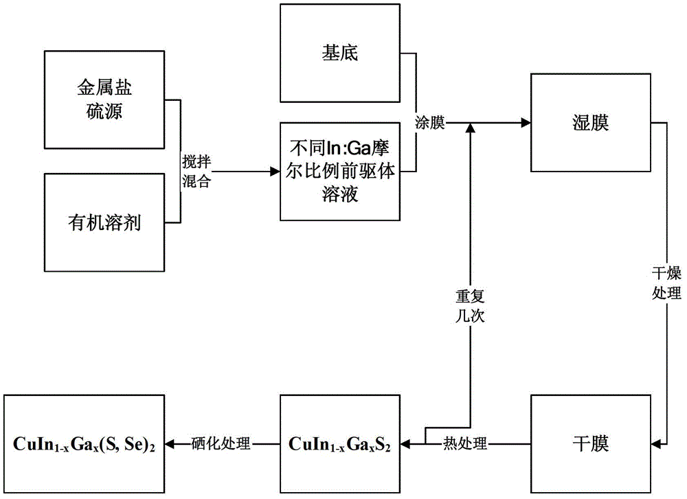
[0029] Such as figure 1 As shown, the copper indium gallium sulfide selenium thin film absorption layer preparation method of the present application, an implementation thereof, comprises the following steps:

[0030] Step 1. Prepare precursor solution:

[0031] Dissolve copper, indium and gallium chloride, acetate or copper acetylacetonate in an organic solvent, add a sulfur source, and stir to obtain a uniform precursor solution, wherein the molar ratio of Cu:In:Ga:S is ( 0.8~1):(0.63~0.8):(0.2~0.37):(2~2.5);

[0032] In one embodiment, copper, indium and gallium chloride, acetate or acetylacetonate can be dissolved in organic solvents such as pyridine, dimethyl sulfoxide, 1-butylamine, and then thiourea or Carbon disulfide is used as a sulfur source, and after stirring at room temperature for 0.5-2 hours, a homogeneous solution is obtained, wherein the molar ratio of Cu:In:Ga:S is (0.8-1):(0.63-0.8):(0.2-0.37):( 2~2.5), the concentration of metal ions is 0.1~0.8mol / L.

...

Embodiment 1

[0047] Copper acetate, indium chloride, gallium acetylacetonate and thiourea are used as raw materials, and the raw materials are weighed according to the Cu:In:Ga:S molar ratio of 1:0.7:0.3:2.2. The weighed raw materials were dissolved in pyridine, and the amount of solvent used was adjusted so that the metal ion concentration was 0.1M. After magnetic stirring for 60 min, a uniform solution with a certain viscosity was obtained. Precursor films were prepared on Mo-coated soda-lime glass by spin coating, and then dried at 200°C for 10 minutes to change the molar ratio of In:Ga. Repeat the above steps several times to obtain a precursor film with a thickness of 1.5-2 μm. . Finally, the precursor film was put into a tube furnace for heat treatment under N2 atmosphere, the heat treatment temperature was 450°C, and the heat treatment time was 15 minutes to obtain CuIn 0.7 Ga 0.3 S 2 film. CuIn 0.7 Ga 0.3 S 2 The film is selenized in a selenization furnace, the selenium sou...

Embodiment 2

[0049] Copper acetate, indium chloride, gallium chloride and thiourea are used as raw materials, and the raw materials are weighed according to the Cu:In:Ga:S molar ratio of 0.9:0.7:0.3:2.2. The weighed raw materials were dissolved in dimethyl sulfoxide solvent, and the amount of solvent was adjusted so that the total concentration of metal ions was 0.8M. After magnetic stirring for 30 min, a uniform and stable solution was obtained. The precursor film was prepared on the Mo-coated soda-lime glass by spin coating, and the subsequent steps were the same as in Example 1 for drying and heat treatment to obtain a CIGS film. Finally, put the film into a selenization furnace for selenization treatment. The selenium source used is solid high-purity Se powder, and the temperature of the selenium source is 230 ° C, N 2 The flow rate is 0.2m 3 / h, the selenization temperature is 400°C, and the selenization time is 30min. After selenization treatment, the CIGSSe thin film is prepared....


PUM

PropertyMeasurementUnit
thicknessaaaaaaaaaa
thicknessaaaaaaaaaa

Abstract

The invention discloses a preparation method of a copper-indium-gallium-sulfur-selenium film absorbing layer. The preparation method comprises the following steps of preparing a precursor solution, preparing a precursor film, carrying out a heat treatment to the precursor film, preparing a CuIn1-xGaxS2 film with Ga in gradient distribution, and carrying out selenization processing to the CuIn1-xGaxS2 film with Ga in gradient distribution in a selenization furnace; and a CuIn1-xGax(S,Se)2 film absorbing layer is obtained. The invention also discloses a copper-indium-gallium-sulfur-selenium film absorbing layer and a cell comprising the same. Because components of the precursor solution are adjustable, Ga can be in gradient distribution in the absorbing layer by means of adjusting the molar ratio of In to Ga in the solution; and at the same time, by means of a volume expansion effect of Se atoms replacing part of S atoms in the selenization process, the structure densification of the copper-indium-gallium-sulfur-selenium film is achieved, and the forbidden band width of the absorbing layer can be adjusted by replacing S atoms by Se atoms.

Description

technical field [0001] The present application relates to the field of solar photovoltaics, in particular to a copper indium gallium sulfide selenide solar cell, a copper indium gallium sulfide selenide thin film absorber layer and a method for preparing a copper indium gallium sulfide selenide thin film absorber layer. Background technique [0002] In recent years, with the continuous consumption of fossil energy and the enhancement of environmental awareness, green renewable energy has become a hot spot for investment and research in various countries, especially the development and utilization of solar energy. The types of solar cells currently on the market include: crystalline silicon solar cells, polycrystalline silicon solar cells, amorphous silicon thin-film solar cells, CdTe thin-film solar cells and copper indium gallium selenide thin-film solar cells (CIGS). Among the above-mentioned thin-film solar cells, copper indium gallium selenium thin-film solar cells have ...

Claims


Application Information

Patent Timeline
Patent Type & Authority Patents(China)
IPC IPC(8): C01B19/00C01G15/00H01L31/18H01L31/032
CPCY02P70/50
Inventor 徐东徐永清汤珅
Owner 徐东
Why Eureka
Try Eureka