Ultra Thin Film Field Effect Transistor Sensor and Its Application

A technology of transistors and sensors, which is applied in the field of ultra-thin film field effect transistor sensors, can solve problems such as unsatisfactory response or selectivity of devices, unfavorable large-scale preparation and application, and harsh technical means, and achieve excellent solution film-forming characteristics, Ease of integration and improved response efficiency

Active Publication Date: 2016-01-13
INST OF CHEM CHINESE ACAD OF SCI
View PDF4 Cites 0 Cited by
  • Summary
  • Abstract
  • Description
  • Claims
  • Application Information

AI Technical Summary

Problems solved by technology

[0005] In recent years, the research on the use of organic thin film transistor (OTFT) devices for gas sensing has attracted people's attention, and some people have used classic organic semiconductor materials, such as α-6-thiophene (α-6T), pentacene, phthalocyanine, etc. Derivatives, poly 3-hexylthiophene (P3HT), etc., are used in the sensing research of ammonia, but the device response or selectivity is not ideal
In 2012, the Katz research group of Johns Hopkins University in the United States used tris(pentafluorophenyl)borane as the signal receiving conversion layer to prepare ammonia sensors (Huang, W.; Besar, K.; LeCover, R.; Rule, A.M.; Breysse, P.N.; Katz, H.E., J.Am.Chem.Soc.2012, 134(36), 14650-14653.), the detection limit concentration reached 0.35ppm, but in the process of transistor device preparation, organic The semiconductor material layer needs copper phthalocyanine or cobalt phthalocyanine and tris(pentafluorophenyl)borane to be delicately co-evaporated with a thickness of 6nm under vacuum conditions, and the technical means are relatively strict.
Although this type of device shows good sensing characteristics, the uniformity between devices is poor due to the discontinuity of the film, which is not conducive to large-scale preparation and application.

Method used


Image

  • Ultra Thin Film Field Effect Transistor Sensor and Its Application
  • Ultra Thin Film Field Effect Transistor Sensor and Its Application
  • Ultra Thin Film Field Effect Transistor Sensor and Its Application

Examples


Embodiment 1

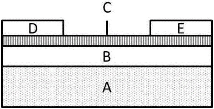
[0066] Prepare the organic field effect transistor sensor according to the following steps:

[0067] 1) Use a silicon wafer with a thickness of 1mm as the gate, and prepare SiO with a thickness of 300nm on the gate layer by thermal oxidation growth method 2 as an insulating layer;

[0068] 2) Prepare the organic sensing layer on the insulating layer obtained in step 1) by shearing and pulling the film. The solvent is toluene, the solution volume is 20 μL, the film pulling speed is 0.15-0.30 mm / s, and the temperature of the silicon wafer is 70 ° C. The experiment was carried out in an open system, and the compound of formula I with the following structure was used as the material of the organic sensing layer:

[0069]

[0070] Formula I1

[0071] Among them, heteroatom X=S, m=2; R 1 =R 2 =-C 6 h 13 ;

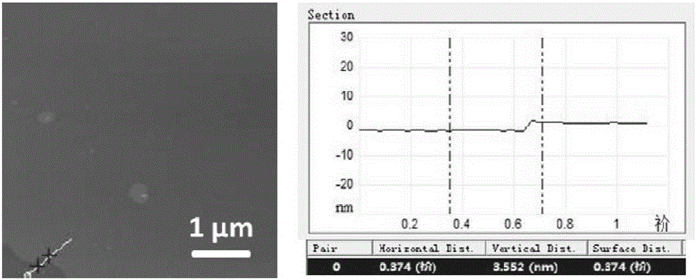
[0072] Such as image 3 As shown in the atomic force microscope photo, the obtained organic sensing layer is uniform and continuous, with a thickness of 3.55nm, whic...

Embodiment 2

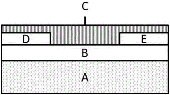
[0089] Prepare the organic field effect transistor sensor according to the following steps:

[0090] 1) Use a silicon wafer with a thickness of 1mm as the gate, and prepare SiO with a thickness of 300nm on the gate layer by thermal oxidation growth method 2 as an insulating layer;

[0091] 2) On the insulating layer obtained in step 1), use vacuum evaporation (vacuum degree is 10 -4 Pa, the evaporation rate is ) method to prepare gold electrodes, respectively as the source electrode and the drain electrode, the thickness is 20nm;

[0092] 3) Prepare an organic sensing layer on the insulating layer obtained in step 2) by spin coating. The solvent used in the spin coating step is tetralin, the spin coating speed is 6000rpm, and the time is 2 to 3min. It is carried out at room temperature. The compound belonging to the formula I of the structure shown in the following formula I2 is used as the material of the organic sensing layer to obtain the organic field effect transistor...

Embodiment 3

[0106] According to the steps of Example 1, only the material of the organic sensing layer is replaced by the compound shown in formula I3;

[0107] Atomic force microscope photo ( Figure 9 ) shows that the thickness of the organic sensing layer is 7.2 nm, which is ~2 molecular layers;

[0108]

[0109] Formula I3

[0110] Among them, heteroatom X=S, m=2; R 1 =R 2 =-OC 6 h 13 ;

[0111] The performance of the transistor sensor obtained in this embodiment is not substantially different from that of embodiment 1 in terms of ammonia detection.


PUM

PropertyMeasurementUnit
thicknessaaaaaaaaaa
thicknessaaaaaaaaaa
thicknessaaaaaaaaaa

Abstract

The invention discloses an ultrathin film field effect transistor and an application thereof. A transistor sensor comprises a grid layer, an insulation layer, an organic sensing layer, a source and drain, and is in the following structure a (a bottom grid top contact type), or the following structure b (a bottom grid bottom contact type), wherein for the structure a, the insulation layer is located above the grid layer, the organic sensing layer is located above the insulation layer, and the source and the drain are located on the same layer and above the organic sensing layer. The organic sensing layer is made of a compound shown as Formula I as shown in the specification. The transistor sensor can make a quick and sensitive sensing response to ammonia at the room temperature, is high in selectivity, restorable, low in manufacturing cost and simple in technology, is one of the most sensitive ammonia sensors at present, facilitates device miniaturization and integration, and is suitable for larger scale production, and a limit of detection of the transistor sensor can reach 0.1ppm.

Description

technical field [0001] The invention relates to the field of organic semiconductor materials and gas detection sensors, in particular to an ultra-thin film field effect transistor sensor and its application. Background technique [0002] Ammonia (NH 3 ) as an important raw material for ammoniation, is widely used in the production of precursors of various chemical products such as nitric acid and urea, pesticides, medicines and fertilizers, and its liquid form (liquid ammonia) is not only an effective industrial refrigerant, It is also widely used in the manufacture of rockets and missile propellants in the fields of national defense and military industry. However, ammonia is a colorless, toxic, and flammable gas with a strong, pungent odour. Short-term exposure to low-concentration ammonia atmosphere can cause poisoning symptoms such as edema in the respiratory tract and gastric mucosa. In severe cases, it can produce neurotoxicity, cause tissue dissolution and necrosis, ...

Claims


Application Information

Patent Timeline
Patent Type & Authority Patents(China)
IPC IPC(8): G01N27/414H01L51/05H01L51/30H01L51/40
Inventor 孟青张凤娇臧亚萍邹业狄重安胡文平朱道本
Owner INST OF CHEM CHINESE ACAD OF SCI
Why Eureka
Try Eureka