

Method for improving carbon nanotube field emitting performance through diamond-like carbon film
A field emission and performance technology, applied in the manufacture of discharge tubes/lamps, electrical components, cold cathode manufacturing, etc., can solve problems such as reducing the field emission threshold voltage
- Summary
- Abstract
- Description
- Claims
- Application Information
AI Technical Summary
Problems solved by technology
Method used
Image

Examples
Embodiment 1
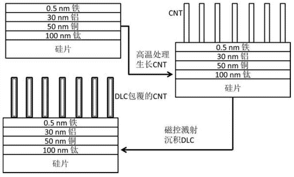
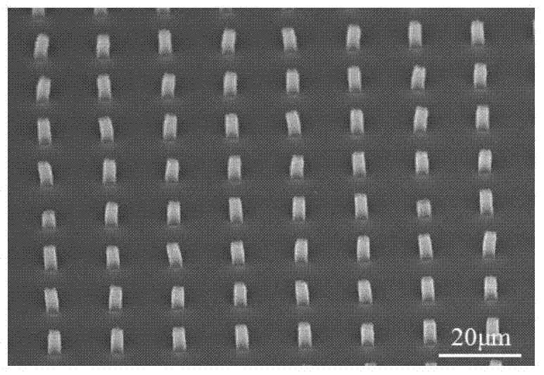
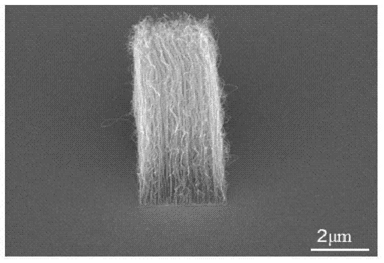
[0052] A kind of method utilizing DLC to improve CNT field emission performance, its basic process is as figure 1 shown, including the following steps:
[0053] (1) Substrate preparation. The silicon wafers were respectively placed in acetone, alcohol, and deionized water for 10 minutes of ultrasonic vibration to remove impurities on the surface of the silicon wafers. Fabricate a patterned array on a clean silicon wafer surface using UV lithography. If the CNT does not require patterned growth, no patterning process is required. Subsequently, 100nm titanium (Ti), 50nm copper (Cu), 30nm aluminum (Al), and 0.5nm iron (Fe) were produced on the surface of the silicon wafer by electron beam evaporation technology to obtain a CNT growth substrate.
[0054] (2) CNT growth. Place the sample in a closed heating system, and first evacuate the system to below 0.1mbar. Then feed 700sccm hydrogen (H 2 ), so that the system pressure is maintained at 30mbar. The temperature of the s...
Embodiment 2
[0057] A method utilizing DLC to improve CNT field emission performance, comprising the following steps:
[0058] (1) Substrate preparation. Place the stainless steel sheet in acetone, alcohol, and deionized water for 10 minutes of ultrasonic vibration to remove impurities on the surface of the stainless steel sheet. Patterned arrays were fabricated on clean stainless steel surfaces using electron beam lithography. If the CNT does not require patterned growth, no patterning process is required. Subsequently, 100nm gold (Au), 50nm graphene, 5nm TiN, and 15nm cobalt (Co) were produced on the surface of the silicon wafer by electron beam evaporation technology to obtain a CNT growth substrate.
[0059] (2) CNT growth. Place the sample in a closed heating system, and first evacuate the system to below 0.1mbar. Then 600 sccm of hydrogen (H2) was fed into the system to keep the system pressure at 1 mbar. The temperature of the system is raised to 600°C for pretreatment for 1 ...
Embodiment 3
[0062] A method utilizing DLC to improve CNT field emission performance, comprising the following steps:
[0063] (1) Substrate preparation. Place the copper sheet in acetone, alcohol, and deionized water for 10 minutes of ultrasonic vibration to remove impurities on the surface of the copper sheet. Fabricate patterned arrays on clean copper surfaces using nanoimprint lithography. If the CNT does not require patterned growth, no patterning process is required. Subsequently, 20nm molybdenum (Mo), 35nm tungsten (W), 12nm ITO, and 11nm ferrocene were produced on the surface of the silicon wafer by electron beam evaporation technology to obtain a CNT growth substrate.
[0064] (2) CNT growth. Place the sample in a closed heating system, and first evacuate the system to below 0.1mbar. Pass into 630sccm hydrogen (H 2 ), so that the system pressure remains at 20mbar. The temperature of the system is raised to 560°C for 6 minutes of pretreatment, and then the temperature of th...
PUM
| Property | Measurement | Unit |
|---|---|---|
| thickness | aaaaa | aaaaa |
| thickness | aaaaa | aaaaa |
| thickness | aaaaa | aaaaa |
Abstract
Description
Claims
Application Information