Composite conductive material of graphene film and metal nanometer structure and preparation method thereof

A metal nanostructure, graphene thin film technology, applied in metal/alloy conductors, nanotechnology for materials and surface science, nanotechnology, etc., can solve difficult to meet the requirements of practical applications, high resistance of conductive materials, affect conduction performance and other issues, to achieve the effects of good light transmittance, excellent electrical conductivity, and simple operation

Active Publication Date: 2015-05-13
ZHEJIANG UNIV
View PDF6 Cites 16 Cited by
  • Summary
  • Abstract
  • Description
  • Claims
  • Application Information

AI Technical Summary

Problems solved by technology

The composite conductive material provided by this invention is synthesized by the chemical solution blending method. Blending in an organic solvent will cause graphene to break and form defects, which will affect the electrical conductivity and easily cause environmental pollution; the graphene preparation process of the invention requires removal of Catalytic layer; in addition, it also leads to high surface resistance of conductive materials, which is difficult to meet the requirements of practical applications

Method used


Image

  • Composite conductive material of graphene film and metal nanometer structure and preparation method thereof
  • Composite conductive material of graphene film and metal nanometer structure and preparation method thereof
  • Composite conductive material of graphene film and metal nanometer structure and preparation method thereof

Examples


Embodiment 1

[0048] Embodiment 1 adopts CVD method to synthesize graphene thin film on copper nanostructure, comprises the following basic steps:

[0049] (1) Copper nanoparticles (about 100nm in particle diameter) are uploaded to the CVD system prepared by graphene;

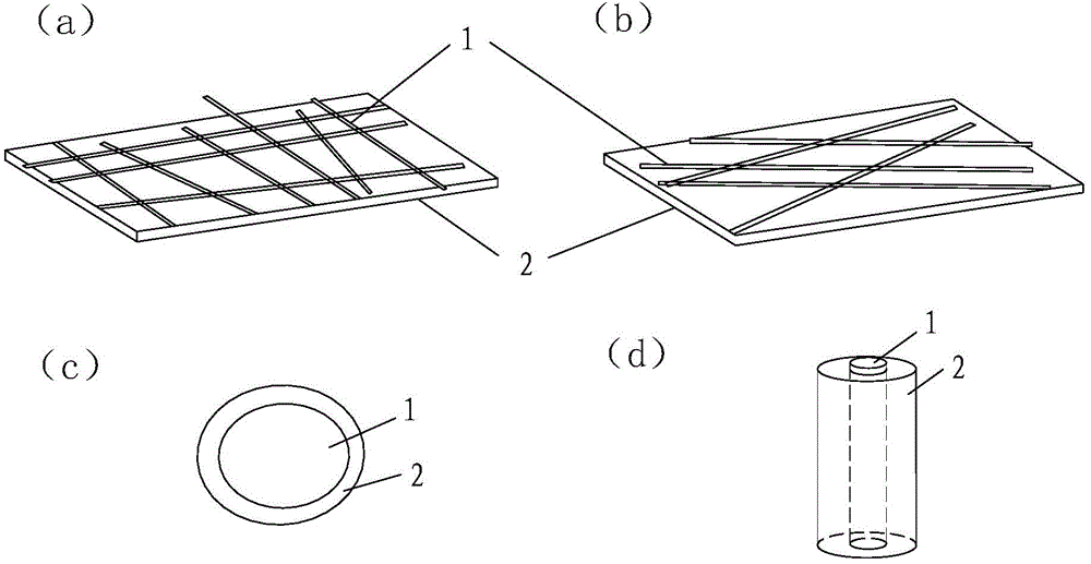
[0050] (2) Using methane gaseous carbon source (H 2 / CH 4 The flow ratio of the graphene film is 20:1) to synthesize a graphene film on the surface of copper nanoparticles, the synthesis temperature is 1030°C, and the synthesis time is 2 hours. Conductive material with core-shell structure, its structure diagram is as follows figure 1 (c) shown.

[0051] The graphene film that embodiment 1 is synthesized is the graphene of 4 layers, also can adjust the experimental parameters such as the time that prepares graphene film, the flow rate of methane and adjust the number of layers of synthetic graphene film according to actual needs. The carbon source for synthesizing graphene film can be gaseous, liquid or even solid carbon...

Embodiment 2

[0052] Embodiment 2 adopts carbon segregation method to synthesize graphene thin film on nickel-copper alloy nanostructure, comprises the following basic steps:

[0053] (1) Ni-Cu nanowires (about 50nm in diameter and about 5000nm in length) are buried in carbon powder with a purity of 85%;

[0054] (2) Treat at a temperature of about 1000°C for 20 hours;

[0055] (3) be cooled to room temperature, carbon atom segregation forms graphene film (thickness about 30 layers of graphene) on the surface of nickel-copper alloy like this, forms nickel-copper: the core-shell structure of graphene film, its structural diagram is as follows figure 1 (d) shown.

[0056] The metal nanostructure that embodiment 2 adopts is nickel-copper alloy nanowire, but also can select other metal nanostructure, as silver, gold, platinum, nickel, aluminum, magnesium, tungsten, ruthenium etc. and their alloy composition, its size scale , shape, etc. can be determined according to actual needs. The graphe...

Embodiment 3

[0057] Embodiment 3 adopts solid-state carbon source method to synthesize graphene thin film on nickel foil, comprises the following basic steps:

[0058] (1) Upload the nickel foil (25 μm in thickness) to the graphene preparation system;

[0059] (2) Prepare a carbon film of about 10nm on the nickel foil, and then in Ar / H 2 Under the atmosphere of the carbon film, the nickel foil deposited with the carbon film was heat-treated for about 40 minutes, and then cooled to room temperature to prepare a graphene film (the number of layers is 3 layers of graphene);

[0060] (3) adopt spin coating method to prepare polymethacrylate (PMMA) support layer on the graphene film of nickel / graphene film, the thickness of support layer is about 500nm;

[0061] (4) Micro-nano processing is carried out to the nickel foil of PMMA / graphene film / nickel, makes nickel foil form the nanostructure of net shape, the nickel band width in the nickel mesh structure is 300nm, thereby prepares PMMA / graphen...


PUM

PropertyMeasurementUnit
sizeaaaaaaaaaa
thicknessaaaaaaaaaa
thicknessaaaaaaaaaa

Abstract

The invention discloses a composite conductive material of graphene film and metal nanometer structure; the composite conductive material of graphene film and metal nanometer structure comprises a metal nanometer structure and a graphene film which sticks onto the metal nanometer structure; the graphene film directly sticks onto the metal nanometer structure by chemical vapor deposition method or carbon segregation method; the layer number of the graphene film is 1-30 layers. The provided conductive material has mechanical flexibility and high conductivity as well as adjustable light transmission; meanwhile, the transparent material also has a characteristic of preventing the metal from being oxidized. The square resistance of the provided conductive material is 5Omega / to 1000Omega / , the transparency is 5%-97%, and the bending radius is less than 10mm. The invention also discloses a preparation method of the conductive material; the provided preparation method of the conductive material does not need to transfer the graphene film; the operation is simple without using an organic solvent; the conductive material and preparation method are green and environment-friendly, as well as saving cost.

Description

technical field [0001] The invention relates to the field of conductive materials, in particular to a conductive material composited with a graphene film and a metal nanostructure and a preparation method thereof. Background technique [0002] Transparent conductive film materials are widely used in optoelectronic devices such as touch screens, various display devices, and solar cells. More than 97% of the transparent conductive films currently on the market are indium tin oxide (ITO) transparent conductive materials containing rare earth metal indium. ITO as a transparent electrode material has high transparency and surface resistance can be as low as 30Ω / □. However, the content of metal indium in the earth's crust is limited, and the cost is increasing year by year; at the same time, ITO has unstable chemical and thermal properties, and mechanical brittleness. The rapid development of wearable optoelectronic devices has put forward higher requirements for transparent cond...

Claims


Application Information

Patent Timeline
Patent Type & Authority Applications(China)
IPC IPC(8): H01B1/04H01B1/02H01B13/00
CPCB82Y30/00B82Y40/00H01B1/02H01B1/04H01B13/00
Inventor 徐明生梁涛
Owner ZHEJIANG UNIV
Why Eureka
Try Eureka