Molybdenum disulfide / silicon heterojunction solar energy cell and preparation method thereof

A technology of solar cells and molybdenum disulfide, applied in circuits, electrical components, photovoltaic power generation, etc., can solve problems such as difficulties, inability to meet large-scale promotion and application, and high cost, and achieve low cost, good application prospects, and high The effect of crystallization properties

Inactive Publication Date: 2016-01-13
HUAZHONG UNIV OF SCI & TECH
View PDF4 Cites 10 Cited by
  • Summary
  • Abstract
  • Description
  • Claims
  • Application Information

AI Technical Summary

Problems solved by technology

For the current silicon-based solar cells, the efficiency is close to the theoretical limit, and it is very difficult to further improve the conversion efficiency; although silicon-based solar cells are the most mature in solar cells, due to the high cost, it is far from possible To meet the requirements of large-scale promotion and application, therefore, the development of solar energy is inseparable from the selection and improvement of semiconductor materials
[0004] Molybdenum disulfide (MoS 2 ) is a natural mineral with abundant reserves, low price, good thermal stability and chemical stability; it has wide band gap and adjustable band gap physical properties in

Method used


Image

  • Molybdenum disulfide / silicon heterojunction solar energy cell and preparation method thereof
  • Molybdenum disulfide / silicon heterojunction solar energy cell and preparation method thereof
  • Molybdenum disulfide / silicon heterojunction solar energy cell and preparation method thereof

Examples


preparation example Construction

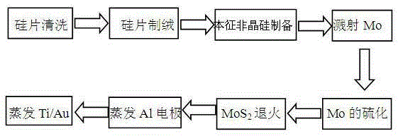
[0033] MoS of the present invention 2 / A method for preparing a Si heterojunction solar cell, comprising the following steps:

[0034] (1) Use acetone solution to ultrasonically clean the single crystal silicon wafer to remove organic dirt on the surface of the silicon wafer, and use alcohol to carry out ultrasonic cleaning to the silicon wafer to remove the acetone on the surface of the silicon wafer, and rinse with deionized water for 3 times , in which the thickness of the monocrystalline silicon wafer is 150 microns to 300 microns, and the resistivity is 0.2Ω·㎝~1.0Ω·㎝;

[0035] (2) Using NH 4 F, the HF mixed solution is used to clean the above-mentioned silicon wafer at normal temperature to remove the surface oxide layer, and then rinse it in deionized water. Wherein the concentration of the ammonium fluoride solution is 35wt%~45wt%, the concentration of the hydrofluoric acid solution is 45wt%~55wt%, and the cleaned single crystal silicon wafer is recorded as single c...

example 1

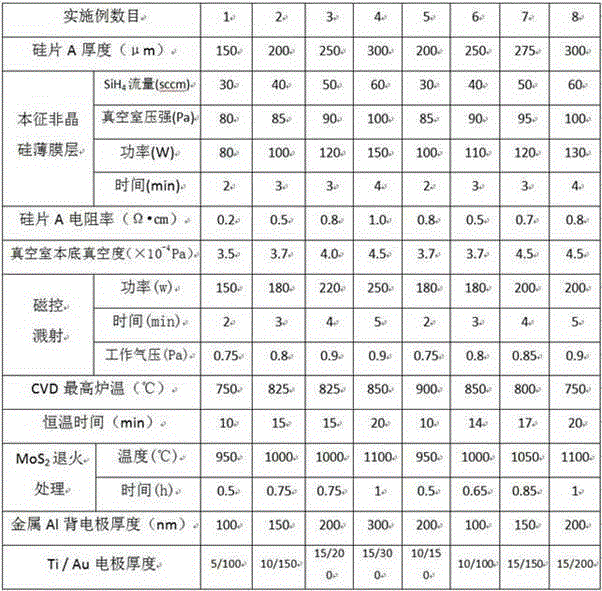
[0050] (1) Complete the basic etching and cleaning of single crystal silicon wafers according to the above scheme, in which the thickness of the silicon wafer is 150 μm, and the resistivity is 0.2Ω·cm;

[0051] (2) SiH is introduced into the PECVD system 4 , flow 30sccm, pressure 80Pa, time 2min, power 80W;

[0052] (3) Magnetron sputtering system pre-evacuation 3.5×10 -4 Pa, high-purity Ar is introduced at 20 sccm, and the pressure of the vacuum chamber is maintained at 0.5 Pa;

[0053] (4) After pre-sputtering, sputter target Mo onto the above-mentioned silicon wafer with a thin layer of amorphous silicon, adjust the sputtering power to 150W, and the sputtering time to 2min;

[0054] (5) When S reacts with metal Mo, the quartz tube is slowly heated to 750°C, kept at a constant temperature for 10 minutes and then cooled;

[0055] (6) Reaction to produce MoS 2 Anneal at 950°C for 0.5h;

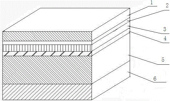
[0056] (7) MoS attached on the upper layer 2 Thermally evaporated Al electrode on th...

example 2

[0059] (1) Complete the etching and cleaning of single crystal silicon wafers according to the above scheme, wherein the thickness of silicon wafers is 200 μm, and the resistivity is 0.5Ω·cm;

[0060] (2) SiH is introduced into the PECVD system 4 , flow 40sccm, pressure 85Pa, time 3min, power 100W;

[0061] (3) Pre-vacuumize the magnetron sputtering system 3.7×10 -4 Pa, high-purity Ar is introduced at 20 sccm, and the pressure of the vacuum chamber is maintained at 0.8 Pa;

[0062] (4) After pre-sputtering, sputter the target material to Mo onto the above-mentioned silicon wafer with a thin layer of amorphous silicon, adjust the sputtering power to 180W, and the sputtering time to 3min;

[0063] (5) When S reacts with metal Mo, the quartz tube is slowly heated to 825°C, kept at constant temperature for 15 minutes and then cooled;

[0064] (6) Reaction to produce MoS 2 Anneal at 1000°C for 0.75h;

[0065] (7) MoS attached on the upper layer 2 Thermally evaporated Al elect...


PUM

PropertyMeasurementUnit
Thicknessaaaaaaaaaa
Resistivityaaaaaaaaaa
Thicknessaaaaaaaaaa

Abstract

The invention discloses a molybdenum disulfide / silicon heterojunction solar energy cell and a preparation method thereof. The chemical vapor deposition method can be used in preparing uniform molybdenum disulfide film with large-area and high crystallinity degree. The molybdenum disulfide film has a relatively high carrier mobility and an adjustable band gap. The prepared molybdenum disulfide / silicon heterojunction solar energy cell has characteristics of normal temperature preparation, simple process, low cost and high photoelectric conversion efficiency, and can perform effective conversion of solar energy even when the cell cost is reduced.

Description

technical field [0001] The invention belongs to the technical field of microelectronics and optoelectronics, and in particular relates to a molybdenum disulfide / silicon heterojunction solar cell and a preparation method thereof. Background technique [0002] With the development of modern industry, the global energy crisis and air pollution problems are becoming more and more serious. As an ideal renewable energy source, solar energy has been valued by many countries. Due to the dual pressure of the reduction of non-renewable energy and environmental pollution, the photovoltaic industry is developing rapidly, and the development of solar cells is also changing with each passing day. Two key issues in the development of solar cells are: improving conversion efficiency and reducing costs. [0003] At present, silicon is the most commonly used material for solar cells. The solar cells made of this material have high conversion efficiency and the technology is relatively mature...

Claims


Application Information

Patent Timeline
IPC IPC(8): H01L31/18H01L31/074
CPCH01L31/074H01L31/18Y02E10/50Y02P70/50
Inventor 曾祥斌陈晓晓文西兴廖武刚王文照徐素娥丁佳
Owner HUAZHONG UNIV OF SCI & TECH
Why Eureka
Try Eureka