Thin barrier enhanced AlGaN/GaN high-electron-mobility transistor and manufacturing method thereof

A high electron mobility and enhanced technology, which is applied in the fields of electrical solid-state devices, semiconductor/solid-state device manufacturing, circuits, etc., can solve the problems of low channel carrier concentration, small transconductance and saturation output current, and poor gate control ability etc. to avoid etching damage and alignment errors, increase saturated output current, and improve breakdown characteristics

Active Publication Date: 2016-09-07
西安电子科技大学重庆集成电路创新研究院
View PDF2 Cites 12 Cited by
  • Summary
  • Abstract
  • Description
  • Claims
  • Application Information

AI Technical Summary

Problems solved by technology

The disadvantages of this enhanced device are: the barrier layer is thinner, the channel carrier concentration is lower, and the saturation current of the device is smaller
The disadvantages of this enhanced device are: the process is complicated, the etching depth is not easy to control accurately, the manufactured device has poor consistency, and the efficiency is low, and it is not easy to prepare large-scale integrated circuits.
The disadvantages of this enhanced device are: poor reliability, easy to cause lattice damage during F plasma treatment, and F ions are easy to diffuse in the barrier layer under high temperature and high field conditions, making the device unstable.
The disadvantages of this enhanced device are: poor gate control ability, the distance between the channel and the gate metal of the device is relatively long, which weakens the control ability of the gate to the channel, and the transconductance and saturation output current are small

Method used


Image

  • Thin barrier enhanced AlGaN/GaN high-electron-mobility transistor and manufacturing method thereof
  • Thin barrier enhanced AlGaN/GaN high-electron-mobility transistor and manufacturing method thereof
  • Thin barrier enhanced AlGaN/GaN high-electron-mobility transistor and manufacturing method thereof

Examples


Embodiment 1

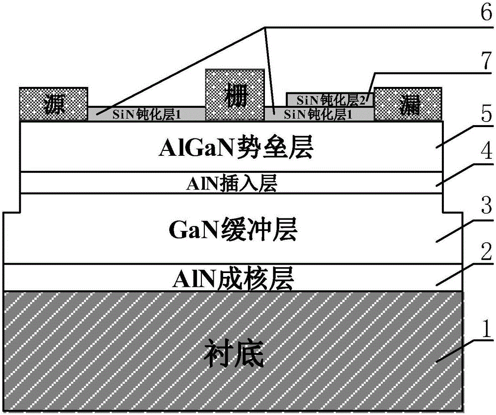
[0039] Example 1, the production substrate is sapphire, the thickness of the first layer of SiN passivation is 2nm, the thickness of the second layer of SiN passivation is 2nm, and the thickness of the AlGaN barrier layer is 3nm. Thin barrier enhanced AlGaN / GaN high electron mobility transistor.

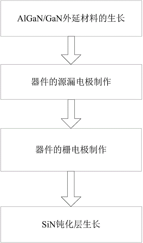
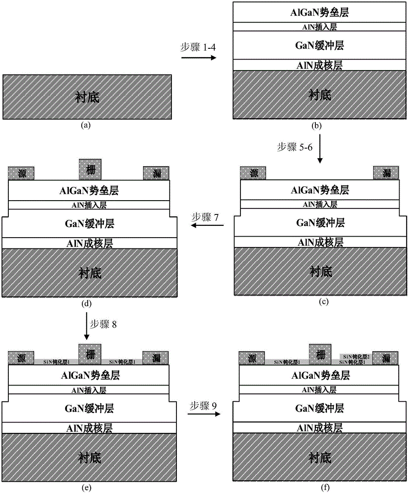
[0040] In step 1, an AlN nucleation layer with a thickness of 20 nm is grown on a sapphire substrate by using a metal oxide chemical vapor deposition (MOCVD) process.

[0041] (1a) Put the sapphire substrate into the reaction chamber of the metal oxide chemical vapor deposition MOCVD equipment; reduce the vacuum degree in the reaction chamber to 1×10 -2 Torr, high-temperature heat treatment and surface nitriding treatment on the sapphire substrate, the treatment conditions are: NH 3 Gas flow rate is 1500sccm, H 2 The gas flow rate is 1500sccm, the heating temperature is 1050°C, the heating time is 5min, and the pressure is maintained at 40Torr;

[0042] (1b) A 20nm thick AlN is gr...

Embodiment 2

[0065] Example 2, the production substrate is SiC, the first layer of SiN passivation thickness is 1.5nm, the second layer of SiN passivation thickness is 2.5nm, and the AlGaN barrier layer thickness is 5nm thin barrier enhanced AlGaN / GaN high electron density Mobility transistor.

[0066] Step 1, growing an AlN nucleation layer on the SiC substrate.

[0067] (1.1) Put the SiC substrate into the reaction chamber of the metal oxide chemical vapor deposition MOCVD equipment; reduce the vacuum degree in the reaction chamber to 1×10 -2 Torr, high-temperature heat treatment and surface nitriding treatment are performed on the SiC substrate, and the treatment conditions are the same as the treatment conditions of step (1a) in embodiment 1.

[0068] (1.2) Deposit and grow AlN with a thickness of 20nm on the SiC substrate as a nucleation layer by metal oxide chemical vapor deposition (MOCVD), and the process conditions are the same as those in step (1b) in Example 1.

[0069] Step 2...

Embodiment 3

[0092] Example 3, the production substrate is sapphire, the thickness of the first layer of SiN passivation is 1nm, the thickness of the second layer of SiN passivation is 3nm, and the thickness of the AlGaN barrier layer is 10nm. Thin barrier enhanced AlGaN / GaN high electron mobility transistor.

[0093] Step A, growing an AlN nucleation layer on the SiC substrate.

[0094] (A1) Put the SiC substrate into the reaction chamber of the metal oxide chemical vapor deposition MOCVD equipment; reduce the vacuum degree in the reaction chamber to 1×10 -2 Torr, high-temperature heat treatment and surface nitriding treatment are performed on the SiC substrate, and the treatment conditions are the same as the treatment conditions of step (1a) in embodiment 1.

[0095] (A2) Deposit and grow AlN with a thickness of 20nm on the SiC substrate as a nucleation layer by metal oxide chemical vapor deposition (MOCVD), and the process conditions are the same as those in step (1b) in Example 1.

...


PUM

PropertyMeasurementUnit
thicknessaaaaaaaaaa
thicknessaaaaaaaaaa
thicknessaaaaaaaaaa

Abstract

The invention discloses a thin barrier enhanced AlGaN / GaN high-electron-mobility transistor device and a manufacturing method thereof, and mainly solves the problems of poor breakdown performance and low output current of the existing similar devices. The technical scheme is that a self-aligned technology is introduced in the SiN passivation layer growth process of the device, and an aligned LDD-HEMT is formed by utilizing the modulation effect of thin and thick SiN passivation layers on channels. The device comprises a substrate, an AlN nucleating layer, a GaN buffer layer, an AlN inserting layer, an AlGaN barrier layer, SiN passivation layers and gate, source and drain electrodes which are arranged from the bottom to the top. There are two SiN passivation layers. After completion of manufacturing of the gate electrode, the first SiN passivation layer is deposited by utilizing the self-aligned effect of the gate electrode, and then the second SiN passivation layer is deposited close to the drain electrode region between the gate electrode and the drain electrode so that the aligned LDD structure is formed. Breakdown voltage and saturation output current of the device are high, and damage introduced in the manufacturing process is low.

Description

technical field [0001] The invention belongs to the technical field of semiconductor devices, in particular to an AlGaN / GaN high electron mobility transistor, which is used as a high-speed device and a high-frequency device. Background technique [0002] GaN material has good electrical properties, such as wide band gap, high breakdown electric field, high thermal conductivity, corrosion resistance, radiation resistance, etc. The third-generation semiconductor material after InP compound semiconductor material is an ideal material for making high-frequency, high-temperature, high-voltage, high-power electronic devices and short-wavelength, high-power optoelectronic devices. At the same time, due to the polarization effect, a high concentration of two-dimensional electron gas will be generated on the heterojunction interface when forming an AlGaN / GaN heterojunction. These characteristics determine that AlGaN / GaN HEMTs will have great application prospects in microwave power. ...

Claims


Application Information

Patent Timeline
Patent Type & Authority Applications(China)
IPC IPC(8): H01L23/29H01L23/31H01L29/778H01L21/335
CPCH01L29/7787H01L23/291H01L23/3171H01L23/3192H01L29/66462
Inventor 曹艳荣何文龙张亚松李鹏戴峰马晓华郝跃郑雪峰吕玲习鹤杨眉毛维许晟瑞
Owner 西安电子科技大学重庆集成电路创新研究院
Why Eureka
Try Eureka