Preparation method of universal chip for detection of protein and nucleic acid by time-of-flight mass spectrometry

A time-of-flight mass spectrometry and chip technology, which is applied in the field of mass spectrometry detection, can solve the problems of low signal-to-noise ratio, single application field, and inability to detect nucleic acid samples across borders.

Inactive Publication Date: 2018-10-19
毅新兴业(北京)科技有限公司
View PDF5 Cites 0 Cited by
  • Summary
  • Abstract
  • Description
  • Claims
  • Application Information

AI Technical Summary

Problems solved by technology

[0017] Although MALDI-TOF time-of-flight mass spectrometry can be used to detect proteins or nucleic acid molecules, from the application point of view, the traditional MALDI chip has a single application field, such as the DE1580TA steel target plate produced by SHIMADZU, which is only used for the identification of protein microorganisms and is suitable for The MALDI-TOF AXIMA of SHIMADZU; the L24 SpectroCHIP chip produced by AGENA is only used for genetic testing and is suitable for AGENA's MALDI-TOF MASSARRY. At present, there is no chip that can cover both genomics testing and proteomics identification.
[0018] From the perspective of the material and surface characteristics of the mass spectrometer chip, the traditional metal chip is repeatedly used, has scratches, and the surface is not chemically modified, the crystal form is poor, the accuracy of the mass spectrometer detection sample peak is low, the signal-to-noise ratio is low, and the baseline high
And for nucleic acid samples, small nucleic acid residues will affect mass spectrometry results
Therefore, metal chips are mainly used for protein spectrum detection, and cannot detect nucleic acid samples across borders.
Nucleic acid chips are mainly made of silicon wafers, but they are expensive, and the matrix formula is monopolized by foreign countries, and the surface of the purchased imported chips has been directly covered with the matrix, which limits their use in protein profiling.

Method used


Image

  • Preparation method of universal chip for detection of protein and nucleic acid by time-of-flight mass spectrometry
  • Preparation method of universal chip for detection of protein and nucleic acid by time-of-flight mass spectrometry
  • Preparation method of universal chip for detection of protein and nucleic acid by time-of-flight mass spectrometry

Examples


Embodiment 1

[0096] Embodiment 1, microarray chip surface hydrophilic treatment

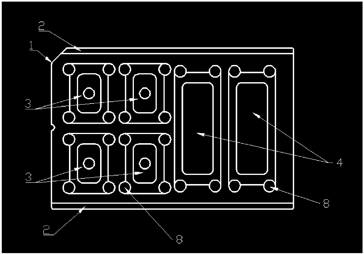
[0097] The main feature of the chip is tough texture and good flatness; diamond, single crystal silicon, quartz crystal, etc.; divided into a sheet structure suitable for the size of the surface unit of the chip adapter, the thickness of the chip is 0.5-1.8mm, in order to ensure the accuracy of quality inspection, the surface of the chip The flatness is less than 10μm. For example, a single crystal silicon wafer is selected as the base of the microarray chip, and silicon dioxide oxide films, zinc oxide films, and aluminum oxide films can be fired and grown on the surface of the silicon wafer structure, with a thickness of 150-800nm, preferably 500nm. Water-based, using thermal oxidation process.

[0098] Such as image 3 As shown, the steps of using a thermal oxidation device to burn and grow a silicon dioxide oxide film are as follows:

[0099] ① Place the silicon wafer in a reaction tube made of quartz g...

Embodiment 2

[0107] Embodiment 2, microarray chip surface hydrophobic treatment

[0108] 1. Sealing treatment of hydrophilic spotting hole area

[0109] Clean residual organic matter on the surface of the chip: first pass the oxygen flow rate of 60-140ml / min, the power of 100-300W, and the treatment time of 1-10min; Thoroughly cleansed and hydroxylated.

[0110] Photoresist technology to seal the sample hole area: Spin the photoresist on the treated substrate by spin coating, the spin coating speed is 1000 ~ 8000rpm, and then place it under the photolithography mask plate, in the 390nm ultraviolet After being exposed to light for 20s~5min, it is eluted with the corresponding developer, so as to construct the spotting hole area with an ordered structure. The photoresist uses acid-resistant polymethyl methacrylate (PMMA) and / or polystyrene.

[0111] 2. Hydrophobic treatment of the outer area of ​​the microarray chip hole

[0112] The process of surface treatment of metal or non-metal mat...

Embodiment 3

[0137] Example 3: Crystallization comparison between microarray dual-purpose chip and traditional chip

[0138] Select the same protein or nucleic acid sample, and take an appropriate amount of the corresponding matrix solution and drop them on the dual-purpose chip and the traditional chip respectively. After the matrix is ​​naturally dried, observe the crystal form under the microscope.

[0139] Such as Figure 5 As shown, the crystal form of the traditional biological detection chip (left picture) is irregular, the thickness is uneven, and it is in the shape of a coffee ring, with a hollow center and thick surroundings. However, the microarray chip provided by the present invention has regular crystal morphology (right picture), uniform thickness, and fine crystal growth.


PUM

PropertyMeasurementUnit
thicknessaaaaaaaaaa
contact angleaaaaaaaaaa
surface smoothnessaaaaaaaaaa

Abstract

The invention provides a preparation method of a general chip for flight time mass spectrometry detection of protein and nucleic acid. The method comprises the steps as follows: (1) a chip with tough texture and good flatness is selected as a substrate or chip body; (2) the chip surface is subjected to hydrophilic treatment; (3) hydrophilic sample application holes are closed with a photoresist; (4) the chip is treated with a silane coupling agent selected from vinylsilane, aminosilane and dimethyldichlorosilane; (5) a sample application area closed with the photoresist is recovered; (6) the chip and a metal chip adapter are matched and mounted, wherein the sample application holes are pretreated with a covering matrix solution in advance, and the matrix solution is selected from a matrix solution for protein mass spectrometry or selected from a matrix solution for nucleic acid mass spectrometry.

Description

technical field [0001] The invention relates to a dual-purpose chip for detecting protein and nucleic acid by time-of-flight mass spectrometry, which can detect protein and nucleic acid molecules by mass spectrometry, and belongs to the field of mass spectrometry detection. Background technique [0002] Proteomics is a new science in the era of functional genomics, which studies the composition, activity rules and protein-protein interactions of intracellular proteins from an overall level. Including the identification of protein expression, modified form, structure, function and interaction. According to the research purpose, proteomics can be divided into expression proteomics, structural proteomics and functional proteomics. Expression proteomics is used to quantitatively study the expression of protein samples in cells. The purpose of proteomics is to map out the structure of protein complexes or proteins present in a special organelle, called structural proteomics, wh...

Claims


Application Information

Patent Timeline
Patent Type & Authority Patents(China)
IPC IPC(8): G01N33/68C12Q1/68
CPCC12Q1/6872G01N33/6848
Inventor 马庆伟梁飞陈莲莲付书辉党文娟
Owner 毅新兴业(北京)科技有限公司
Why Eureka
Try Eureka