
Capacitor, capacitor-burying circuit board and manufacturing method thereof

A technology of capacitors and conductive materials, applied in the manufacture of multilayer circuits, including printed capacitors, including printed electrical components, etc., can solve the problem of small peel strength, easy peeling and bending, application limitations in the field of buried capacitors, and copper electrode thickness. Reduce and other problems to achieve the effect of expanding the number of applications, avoiding the peeling of the laminated copper foil, and reducing the number of pinholes

Pending Publication Date: 2017-10-03
RICHVIEW ELECTRONICS CO LTD
View PDF6 Cites 5 Cited by
  • Summary
  • Abstract
  • Description
  • Claims
  • Application Information

AI Technical Summary

Problems solved by technology

The screen printing process is simple and low-cost, but the embedded capacitance value produced has a large dispersion and the accuracy control of the capacitance value is poor
[0010] 2) Thin-film dielectric method below 1 μm: It has been reported that sputtering, CVD, anodic oxidation and other methods are used to attach insulating high-Dk dielectrics below 1 μm (generally inorganic ceramic materials) to thick copper foil or semiconductor silicon wafers, close to 800 ºC high temperature Calcined, the thickness of the thin insulating medium is reduced to the extreme, and then another metal electrode is made; this process can significantly increase the capacitance due to the thin dielectric, but because the dielectric layer is too thin, the processability and reliability are poor (The high-temperature calcination of the dielectric thin layer is easy to produce fine cracks or bubbles, the capacitor is easy to leak current, and the insulation withstand voltage performance is reduced), and the application in the field of buried capacitors is limited.
This process mostly utilizes the strong adhesion between epoxy resin and copper foil, and adds high Dk inorganic particles (BaTiO3, etc.) Peeling or blistering during lamination of copper foil, or increased brittleness of the material, resulting in poor processability of subsequent circuit boards
In addition, in order to avoid wrinkling of the copper surface, the lamination process must use copper foil of 18 μm or more, which makes it difficult to control the area tolerance of the capacitor electrode and affects the control accuracy of the actual capacitance value (the general capacitance value control accuracy is between 5- 10%); on the other hand, the electrodes of thick copper foil are buried in the package substrate, which increases the overall thickness of the package substrate or semiconductor package, which is not conducive to the development trend of thin plate design in the future
There is a way to reduce the thickness of buried capacitor copper foil is to use carrier copper foil, mainly 18μm copper foil or other materials as the carrier to ensure rigidity, 2-5μm thin copper foil is attached to the carrier, and the carrier is peeled off after lamination, leaving Thin copper is used to make copper electrodes; this kind of carrier thin copper foil is very expensive, and it is still difficult to overcome the problem of large roughness of laminated copper foil and poor insulation reliability under the condition of thin insulating medium
[0012] 4) Sputtering method: Etch the copper electrode on the inner core board of the circuit board as the "lower layer copper electrode" of the buried capacitor; on its "lower layer copper electrode", use 3D spraying method to spray to form a dielectric material (such as high Dk Ink), and then sputter target Ni and other metals on the dielectric material, and paste dry film pattern transfer, etching, etc., to form an "upper copper electrode" with a thinner copper thickness; this method only reduces the thickness of the copper electrode on one side, reducing the The effect of the total thickness of the buried capacitor on the circuit board is limited; and the production is cumbersome and the process is too long, it is difficult to overcome the shortcomings of too many pinholes on the surface of the sputtered copper electrode, unstable capacitance performance, and small peel strength, easy to peel and bend and other issues, therefore, the process method is difficult to be widely used in the market

Method used

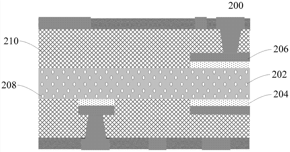
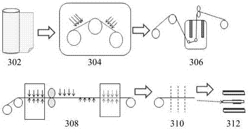

Image

  • Capacitor, capacitor-burying circuit board and manufacturing method thereof
  • Capacitor, capacitor-burying circuit board and manufacturing method thereof
  • Capacitor, capacitor-burying circuit board and manufacturing method thereof

Examples


Embodiment 1

[0100] Substrate components: 20% epoxy resin, BaTiO 3 80%

[0101] Resin thickness: 15 microns

[0102] Dielectric constant: 20, much lower than 35 of similar materials in the prior art

[0103] Dielectric loss factor: 0.009, far lower than 0.014 of similar materials in the prior art.

[0104] First, ion-implant nickel into the substrate, and then conduct plasma deposition of nickel-copper (10-90) alloy to form a metal layer, thereby obtaining a capacitor. The capacitance of the final capacitor is 35, and its performance is more than 50% higher than that of ordinary capacitors.

Embodiment 2

[0106] Substrate components: 15% PI resin, 85% high dielectric constant filler

[0107] Resin thickness: 10 microns

[0108] Dielectric constant: 15, much lower than 40 of similar materials in the prior art

[0109] Dielectric loss factor: 0.010, far lower than 0.029 of similar materials in the prior art.

[0110] Firstly, ion-implanting nickel-chromium alloy into the base material, then depositing nickel by magnetron sputtering, and then depositing copper by magnetron sputtering to prepare a metal layer, thereby obtaining a capacitor. The electrostatic capacitance of the final capacitor is 25, and its performance exceeds that of ordinary capacitors by more than 80%.

Embodiment 3

[0112] Substrate composition: 15% epoxy resin, 85% high dielectric constant filler

[0113] Resin thickness: 20 microns

[0114] Dielectric constant: 15, much lower than 40 of similar materials in the prior art

[0115] Dielectric loss factor: 0.010, far lower than 0.047 of similar materials in the prior art.

[0116] Firstly, ion-implanting nickel-chromium alloy into the base material, then depositing nickel by magnetron sputtering, and then depositing copper by magnetron sputtering to prepare a metal layer, thereby obtaining a capacitor. The electrostatic capacitance of the final capacitor is 30, and its performance exceeds that of ordinary capacitors by more than 90%.

[0117] IX. Conclusion

[0118] The invention can realize metallization on the high dielectric constant polymer substrate with a dielectric constant particle content of more than 80%, and the prepared metal layer and the substrate have high peel strength. Compared with the magnetron sputtering method or p...


PUM

PropertyMeasurementUnit
thicknessaaaaaaaaaa
thicknessaaaaaaaaaa
thicknessaaaaaaaaaa

Abstract

The invention relates to a capacitor, a capacitor-burying circuit board and a manufacturing method thereof. The capacitor comprises a high dielectric constant polymer composite material layer; an ion injection layer, wherein the ion injection layer is formed by injecting the conducting material ion into the high dielectric constant polymer composite material layer at high-speed through an ion injection way; and a metal layer formed and covered on the ion injection layer.

Description

technical field [0001] The invention relates to a capacitor, a buried capacitor circuit board and a manufacturing method thereof. Background technique [0002] As electronic products tend to be light and thin, high-frequency and multi-functional, the degree of circuit integration is getting higher and higher, and the corresponding integrated circuit pins and circuit layouts are increasing, resulting in increased noise. In order to eliminate noise or do electrical compensation, passive devices can be added to the semiconductor package structure to eliminate noise and stabilize the circuit. For example, capacitors have the function of storing charges, which can absorb high-frequency noise in the form of energy temporary storage, thereby reducing system power fluctuations and ensuring the integrity of signal transmission. [0003] One way to increase capacitance is to use SMT surface mount technology to integrate passive components on the substrate, but it is prone to impedanc...

Claims


Application Information

Patent Timeline
Patent Type & Authority Applications(China)
IPC IPC(8): H05K1/16H05K3/46
CPCH05K1/162H05K3/46
Inventor 张志强张晓峰宋红林白四平
Owner RICHVIEW ELECTRONICS CO LTD
Learn More