Silicon-based lithium niobate high-speed light modulator and preparation method thereof

A silicon-based lithium niobate, optical modulator technology, applied in the field of optical communication, can solve the theoretical upper limit of nonlinear electro-optical effect of high cost and temperature sensitive silicon optical modulators, difficult to achieve heterogeneous integration or monolithic integration, devices Drive voltage increase and other issues, to achieve high stability, high bandwidth, reduce the effect of drive voltage

Inactive Publication Date: 2018-11-02
天津领芯科技发展有限公司
View PDF5 Cites 30 Cited by
  • Summary
  • Abstract
  • Description
  • Claims
  • Application Information

AI Technical Summary

Problems solved by technology

[0005] (1) The low electro-optical modulation efficiency of existing lithium niobate high-speed optical modulators makes the driving voltage of the device higher, especially when multiple MZ modulators are connected in parallel to construct coherent optical modulators such as PM-QPSK, the device's The driving voltage will increase significantly;
[0006] (2) The existing lithium niobate high-speed optical modulator has to increase the length of the traveling wave electrode to reduce the driving voltage of the device, but this undoubtedly increases the volume of the device;
[0007] (3) It is difficult to prepare lithium niobate crystals on semiconductor wafers such as gallium arsenide or silicon by coating technology, making it difficult to achieve heterogeneous integration or monolithic integration of lithium niobate and lasers, photodetectors and other structures
However, the high cost and temperature sensitivity of indium phosphide optical modulators, the nonlinear electro-optic effect of silicon optical modulators, and the theoretical upper limit of 60 GHz modulation bandwidth also limit the wide application of these two new optical modulator technologies.

Method used


Image

  • Silicon-based lithium niobate high-speed light modulator and preparation method thereof
  • Silicon-based lithium niobate high-speed light modulator and preparation method thereof
  • Silicon-based lithium niobate high-speed light modulator and preparation method thereof

Examples


Embodiment 1

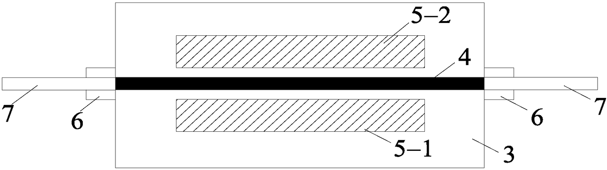
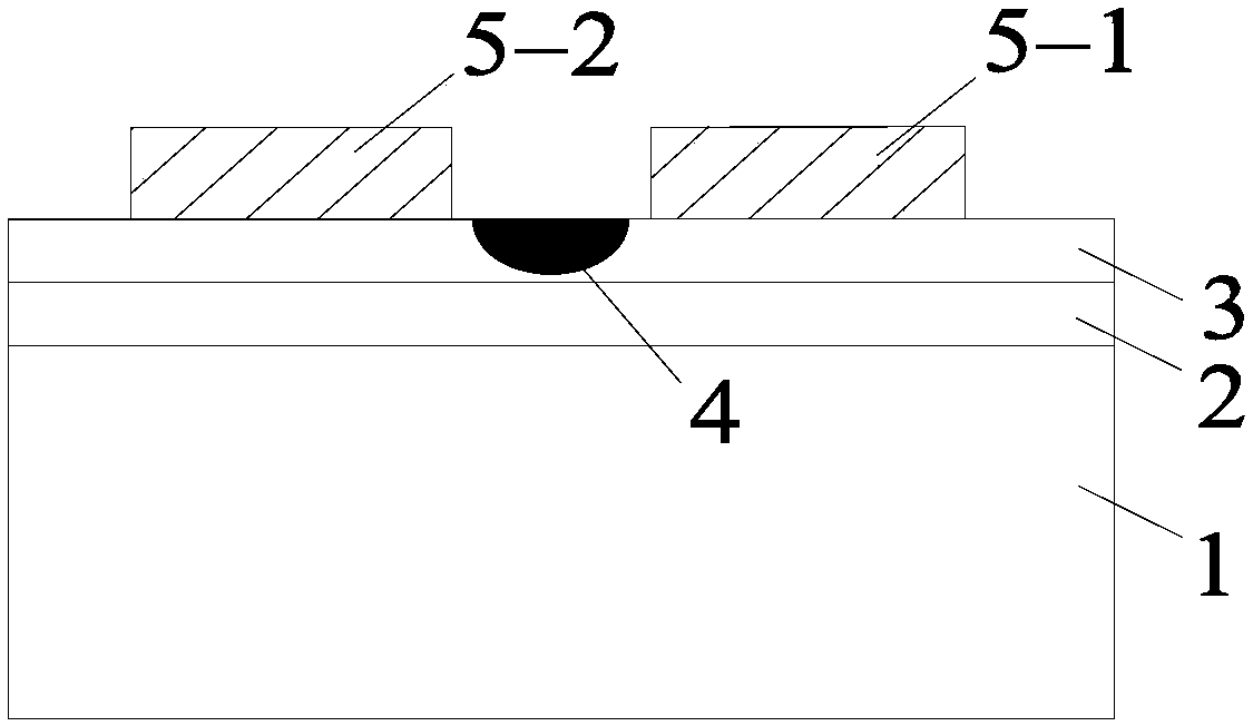
[0058] Such as figure 1 with figure 2 As shown, the silicon-based lithium niobate high-speed light modulator in this embodiment includes: a silicon substrate wafer 1, a silicon dioxide under-cladding layer 2, a lithium niobate film 3, an optical waveguide 4, a metal electrode 5, The signal electrode 5-1, the ground electrode 5-2, the silicon V-groove 6, and the coupling optical fiber 7. The silicon-based lithium niobate high-speed optical modulator in this embodiment is a phase modulator, figure 1 Shown is the structure diagram of a silicon-based lithium niobate high-speed optical modulator, figure 2 Shown is a schematic cross-sectional view of the chip of a silicon-based lithium niobate high-speed light modulator.

[0059] The silicon base wafer 1 uses a single crystal silicon wafer with a [100] crystal orientation and low resistivity, with a thickness ranging from 0.1 mm to 2 mm. The crystal orientation of the silicon substrate wafer 1 is kept consistent with the crystal orien...

Embodiment 2

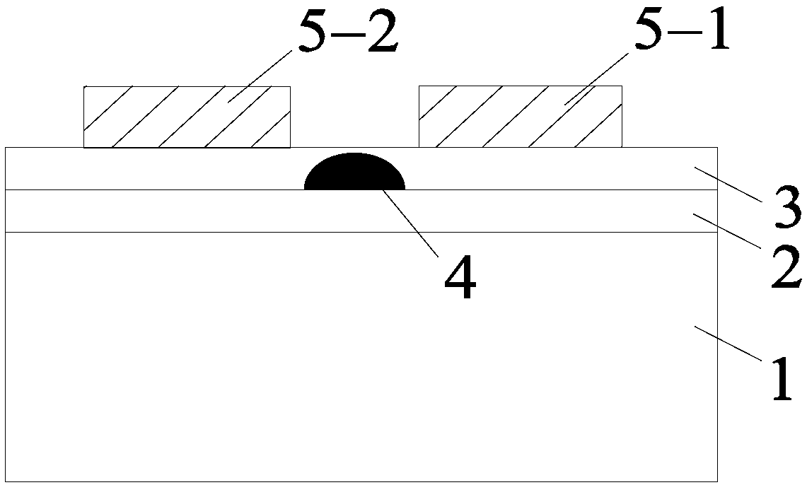
[0078] Such as figure 1 with image 3 As shown, the difference between this embodiment and the silicon-based lithium niobate high-speed optical modulator described in Embodiment 1 is that the optical waveguide 4 used in this embodiment is a titanium diffused optical waveguide. The technical solution of this embodiment is basically the same as that of embodiment 1, except that the optical waveguide 4 in embodiment 1 is changed from annealed proton exchange optical waveguide to a titanium diffused optical waveguide. The detailed technology will not be described here. Program.

[0079] In order to prepare the above-mentioned silicon-based lithium niobate high-speed optical modulator, this embodiment provides a method for preparing a silicon-based lithium niobate high-speed optical modulator including the following steps:

[0080] (1) On the upper surface of the silicon base wafer 1, a thermal oxidation process or any coating technology such as ion sputtering technology, magnetron sput...

Embodiment 3

[0090] Such as Figure 4 with Figure 5 As shown, the main difference between this embodiment and the silicon-based lithium niobate high-speed light modulator described in Embodiment 1 is that this embodiment is an intensity modulator. The specific differences between this embodiment and Embodiment 1 are:

[0091] First, the optical waveguide 4 adopts an MZ-type optical waveguide, which is composed of an input waveguide 4-1, a Y branch structure waveguide 4-2, a double-arm waveguide 4-3, and an output waveguide 4-4. The optical waveguide 4 is made of lithium niobate film Among them, the waveguide width is 1 μm to 10 μm, and the waveguide depth is 1 μm to 10 μm;

[0092] Second, the metal electrode 5 adopts a traveling wave electrode structure, which is composed of a signal electrode 5-1 and two ground electrodes 5-2, and is placed on the left, middle, and right sides of the dual-arm waveguide 4-3. The metal electrode 5 is fabricated on the upper surface of the lithium niobate film...


PUM

PropertyMeasurementUnit
thicknessaaaaaaaaaa
thicknessaaaaaaaaaa
thicknessaaaaaaaaaa

Abstract

The invention discloses a silicon-based lithium niobate high-speed light modulator and a preparation method thereof. The modulator comprises a silicon substrate wafer, a lower silicon dioxide cladding, lithium niobate film, an optical waveguide, a metal electrode, a silicon V-shaped groove and a coupling optical fiber, wherein the lower silicon dioxide cladding is located on the upper surface of the silicon substrate wafer, and the lithium niobate film is located on the lower silicon dioxide cladding. The silicon-based lithium niobate high-speed light modulator has the advantages that heterogeneous integration of a lithium niobate single crystal body and a silicon single crystal body is achieved; by utilizing the thin-film lithium niobate wafer and the characteristics such as low dielectric constant and low dielectric loss of the lower silicon dioxide cladding, improvement of modulation rate (or modulation bandwidth) of the lithium niobate light modulator can be achieved; by utilizingthe thin-film lithium niobate wafer and the high insulativity of the lower silicon dioxide cladding, intensity increase of microwave electromagnetic fields distributed in the lithium niobate film canbe achieved, the modulation efficiency of electric fields to light fields is improved, and the driving voltage of the modulator is reduced.

Description

Technical field [0001] The invention belongs to the technical field of optical communication, and particularly relates to a silicon-based lithium niobate high-speed optical modulator and a preparation method thereof. Background technique [0002] In recent years, with the widespread application of optical communication technology in traditional services such as broadband networks, mobile communications, financial transactions, and data centers, as well as emerging services such as cloud computing, big data, and 5G communications, traditional technologies have improved the speed, capacity, and delay of communications. It has been difficult to meet the needs of people's daily life. Therefore, communication operators are increasingly adopting coherent processing technologies in the architecture of optical networks to realize the establishment of optical transport networks with high speed, large capacity, low delay, and low energy consumption. [0003] In the coherent processing techn...

Claims


Application Information

Patent Timeline
Patent Type & Authority Applications(China)
IPC IPC(8): G02F1/03G02F1/035
CPCG02F1/0305G02F1/0316G02F1/0327G02F1/035
Inventor 李萍范宝泉刘丹姜绍志
Owner 天津领芯科技发展有限公司
Why Eureka
Try Eureka