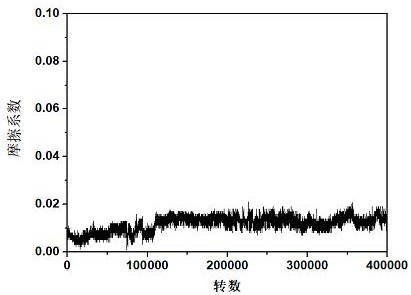
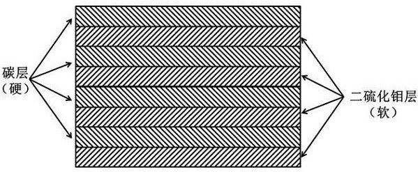
A method for preparing sub-10 nanometer-scale biomimetic structure molybdenum disulfide-carbon multilayer film
A technology of molybdenum disulfide and multi-layer film, which is applied in coating, metal material coating process, vacuum evaporation plating, etc., can solve the problem of low friction coefficient and wear resistance, poor bearing capacity and high wear rate of molybdenum disulfide film and other problems, to achieve the effect of improving uniformity and consistency, improving film/substrate binding force, and increasing plasma density
- Summary
- Abstract
- Description
- Claims
- Application Information
AI Technical Summary
Problems solved by technology
Method used
Image
Examples
Embodiment 1
[0021] Example 1 The single crystal silicon wafer was ultrasonically cleaned with acetone for 10 minutes in a cleaning device. 2 Dry, and then put it into the vacuum chamber; first use the mechanical pump to pump the vacuum chamber to 800Pa, then turn on the Roots pump to pump the vacuum chamber to 10Pa, and then turn on the molecular pump and the low-temperature water vapor pump to pump the vacuum degree of the vacuum chamber to 1.0× 10 -3 Pa; pass 100sccm of Ar gas with a purity greater than 99.99%, and the air pressure is 0.60Pa; turn on the high-voltage ion source power supply, and adjust the high-voltage ion source current to 4A; the high-voltage ion source voltage is 5000V, and the bombardment time is 15min; remove the parts to be plated Oxidation (passivation) layer, dirt and burrs on the surface, that is, the processed base part.
[0022] The Ar gas with a purity greater than 99.99% of 80sccm was introduced, and the treated base member was bombarded with high-energy m...
Embodiment 2
[0029] Example 2 The single crystal silicon wafer was ultrasonically cleaned with acetone in a cleaning device for 10 minutes. 2 Dry, and then put it into the vacuum chamber; first use the mechanical pump to pump the vacuum chamber to 800Pa, then turn on the Roots pump to pump the vacuum chamber to 10Pa, and then turn on the molecular pump and the low-temperature water vapor pump to pump the vacuum degree of the vacuum chamber to 1.0× 10 -3 Pa; inject 100sccm Ar gas with a purity greater than 99.99%, and the air pressure is 0.50Pa; turn on the high-voltage ion source power supply, and adjust the high-voltage ion source current to 3A; the high-voltage ion source voltage is 3000V, and the bombardment time is 15min; remove the parts to be plated Oxidation (passivation) layer, dirt and burrs on the surface, that is, the processed base part.
[0030] The Ar gas with a purity greater than 99.99% of 80sccm was introduced, and the treated base member was bombarded with high-energy mo...
Embodiment 3
[0032] Example 3 The single crystal silicon wafer was ultrasonically cleaned with acetone in a cleaning device for 10 minutes. 2 Dry, and then put it into the vacuum chamber; first use the mechanical pump to pump the vacuum chamber to 800Pa, then turn on the Roots pump to pump the vacuum chamber to 10Pa, and then turn on the molecular pump and the low-temperature water vapor pump to pump the vacuum degree of the vacuum chamber to 1.0× 10 -3 Pa; pass 100sccm of Ar gas with a purity greater than 99.99%, and the air pressure is 0.80Pa; turn on the high-voltage ion source power supply, and adjust the high-voltage ion source current to 5A; the high-voltage ion source voltage is 4000V, and the bombardment time is 15min; remove the parts to be plated Oxidation (passivation) layer, dirt and burrs on the surface, that is, the processed base part.
[0033] Enter 80sccm of Ar gas with a purity greater than 99.99%, first use a high-power pulsed magnetron sputtering power supply to bombar...
PUM
| Property | Measurement | Unit |
|---|---|---|
| hardness | aaaaa | aaaaa |
| elastic modulus | aaaaa | aaaaa |
| friction coefficient | aaaaa | aaaaa |
Abstract
Description
Claims
Application Information


