Perovskite photovoltaic cell based on P-type Au@Cu2-xS interface passivation layer material

A photovoltaic cell, passivation layer technology, applied in nanotechnology for materials and surface science, photovoltaic power generation, nanotechnology for information processing, etc., can solve difficult chlorobenzene dispersion, inability to perovskite/holes problems such as passivation of the interface between the transport layers, to achieve the effects of inhibiting diffusion, promoting charge separation and extraction, and improving fill factor

Active Publication Date: 2020-10-30
WUHAN INSTITUTE OF TECHNOLOGY
View PDF4 Cites 0 Cited by
  • Summary
  • Abstract
  • Description
  • Claims
  • Application Information

AI Technical Summary

Problems solved by technology

However, Au@Cu synthesized according to the method reported in the existing literature (Adv.Funct.Mater.2020,30(12):1908408) 2-x S materials are agglomerated, difficult to disperse in chlorobenzene, and unable to passivate the interface between the perovskite / hole transport layer

Method used


Image

  • Perovskite photovoltaic cell based on P-type Au@Cu2-xS interface passivation layer material
  • Perovskite photovoltaic cell based on P-type Au@Cu2-xS interface passivation layer material
  • Perovskite photovoltaic cell based on P-type Au@Cu2-xS interface passivation layer material

Examples


Embodiment 1

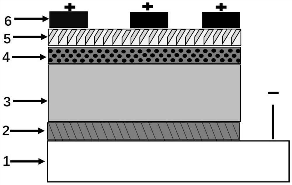
[0047] A planar structure perovskite photovoltaic cell, the structure schematic diagram is as follows figure 2 As shown, its structure includes a transparent conductive substrate 1, an electron transport layer 2, a perovskite photosensitive active layer 3, an interface passivation layer 4, a hole transport layer 5 and a metal electrode 6 from bottom to top, and its preparation method includes the following steps :

[0048] (1) Treatment of transparent conductive substrate: cleaning FTO (fluorine-doped SnO 2 ) conductive glass sheet, first soak the conductive glass sheet in a solution containing detergent for 30 minutes, then rinse it with clean water after repeated scrubbing; then polish it with polishing powder; then put it into deionized water, acetone Ultrasonic for 20 minutes respectively in the container of alcohol and alcohol; finally put in deionized water to rinse twice, blow dry with nitrogen gun and dry in an oven at 80°C;

[0049] (2)SnO 2 QD thin film preparat...

Embodiment 2

[0067] A planar structure perovskite photovoltaic cell comprises a transparent conductive substrate, an electron transport layer, a perovskite photosensitive active layer, an interface passivation layer, a hole transport layer and a metal electrode, and its preparation method comprises the following steps:

[0068] (1) cleaning ITO conductive glass sheet: with embodiment 1;

[0069] (2)SnO 2 Film preparation: SnCl 2 2H 2 O was dissolved in ethanol, coated on the ITO conductive substrate by spin coating method, and annealed at 180 °C for 1 hour in air to prepare SnO 2 film, and put it into a UV-ozone cleaner, and treat it with UV-ozone for 15 minutes in an atmospheric atmosphere and at room temperature, and the treated SnO 2 / ITO substrate is quickly transferred into the glove box;

[0070] (3) Preparation of perovskite photosensitive active layer: same as Example 1;

[0071] (4) Prepare an interface passivation layer on the perovskite photosensitive film:

[0072] a. Au@...

Embodiment 3

[0084] A planar structure perovskite photovoltaic cell comprises a transparent conductive substrate, an electron transport layer, a perovskite photosensitive active layer, an interface passivation layer, a hole transport layer and a metal electrode, and its preparation method comprises the following steps:

[0085] (1) cleaning FTO conductive glass sheet: with embodiment 1;

[0086] (2)SnO 2 Preparation of QD film: same as Example 1;

[0087] (3) Preparation of perovskite photosensitive active layer: same as Example 1;

[0088] (4) Prepare an interface passivation layer on the perovskite photosensitive film:

[0089] a. Au@Cu with core-shell structure 2-x Preparation of S nanoparticles:

[0090] ① Prepare 0.10mol / L CTAB solution and 5mmol / L HAuCl respectively 4 Solution, 15mmol / L NaBH 4 Solution, AA solution of 15mmol / L, NaOH solution of 1.0mmol / L, hexamethylenetetramine solution of 0.1mol / L, thioacetamide solution of 0.1mol / L, copper nitrate solution of 0.1mol / L, spar...


PUM

PropertyMeasurementUnit
thicknessaaaaaaaaaa
particle diameteraaaaaaaaaa
thicknessaaaaaaaaaa

Abstract

The invention relates to a perovskite photovoltaic cell based on a P-type Au@Cu2-xS interface passivation layer material and a preparation method thereof. The cell structurally comprises a transparentconductive substrate, an electron transport layer, a perovskite photosensitive active layer, an interface passivation layer, a hole transport layer and a metal electrode from bottom to top, the interface passivation layer is a coating of Au@Cu2-xS nanoparticles of a core-shell structure, and the thickness of the coating ranges from 20 nm to 150 nm. According to the perovskite photovoltaic cell and the preparation method, the Au@Cu2-xS material with good dispersity and the core-shell structure is prepared by a solution method; the perovskite solar cell is embedded into a hole transport layer / photosensitive layer interface of the perovskite photovoltaic cell; an Au@Cu2-xS near-infrared region is utilized to show relatively strong dual surface plasma resonance absorption characteristics, sothat the absorption spectrum range of a photovoltaic device is widened, the hole density at the interface is remarkably improved, the charge separation and extraction are effectively promoted, and theenergy conversion efficiency of the cell is improved.

Description

technical field [0001] The invention belongs to the technical field of photovoltaic cells, in particular to a P-type Au@Cu based on double surface plasmon resonance 2-x Perovskite photovoltaic cell of S interface passivation layer material and preparation method thereof. Background technique [0002] Perovskite solar cells (PSCs) have the advantages of simple preparation process, low cost, adjustable bandgap width of perovskite semiconductor materials, large light absorption coefficient, long carrier diffusion length, high charge carrier mobility and The advantages of high energy conversion efficiency have rapidly become one of the most promising candidates for the next generation of photovoltaic devices, which has attracted more and more researchers' attention (Y.Zou, Y.Liang, C.Mu, J.P.Zhang, Advanced Materials Interfaces 2019.). Currently, the battery conversion efficiency (PCE) can reach up to 25.2% (Best Research-Cell Efficiencies chart, https: / / www.nrel.gov / pv / assets...

Claims


Application Information

Patent Timeline
Patent Type & Authority Applications(China)
IPC IPC(8): H01L51/44H01L51/42H01L51/48B82Y40/00B82Y10/00B82Y30/00
CPCB82Y10/00B82Y30/00B82Y40/00H10K30/10H10K30/88Y02E10/549Y02P70/50
Inventor 秦平力吴彤王正春肖岚余雪里马良熊伦陈相柏
Owner WUHAN INSTITUTE OF TECHNOLOGY
Why Eureka
Try Eureka