
Preparation method of multi-layer thin film passivation contact structure and full-passivation contact crystalline silicon solar cell

A contact structure, multi-layer thin film technology, applied in the field of solar cells, can solve the problems of narrow annealing process window and small band gap of polysilicon film, and achieve the effect of widening the annealing process window, large energy band bending, and enhancing passivation effect.

Active Publication Date: 2021-09-17
HEBEI UNIVERSITY
View PDF8 Cites 1 Cited by
  • Summary
  • Abstract
  • Description
  • Claims
  • Application Information

AI Technical Summary

Problems solved by technology

[0005] One of the purposes of the present invention is to provide a method for preparing a multilayer thin film passivation contact structure, so as to solve the problems of small band gap and narrow annealing process window of the polysilicon film in the conventional passivation contact structure

Method used

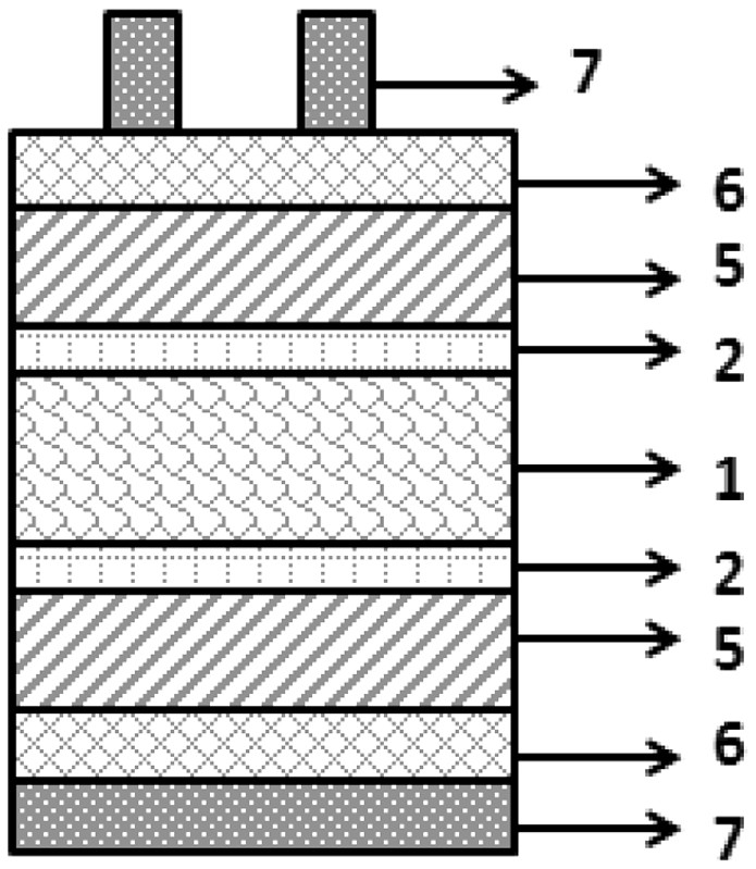

Image

  • Preparation method of multi-layer thin film passivation contact structure and full-passivation contact crystalline silicon solar cell
  • Preparation method of multi-layer thin film passivation contact structure and full-passivation contact crystalline silicon solar cell
  • Preparation method of multi-layer thin film passivation contact structure and full-passivation contact crystalline silicon solar cell

Examples


Embodiment 1

[0028] Such as figure 1 As shown, the present embodiment provides a P-type double-sided multilayer film passivation contact structure, and its structure before annealing is: Boron Doped nc-SiOx:H / Intrinsic nc-SiOx:H / SiOx / c-Si ( P) / SiOx / Intrinsic nc-SiOx:H / Boron Doped nc-SiOx:H; after annealing, its structure is: P + poly-SiOx / SiOx / c-Si (P) / SiOx / P + poly-SiOx. A P-type Czochralski monocrystalline silicon wafer is used as a crystalline silicon substrate 1 with a thickness of 200 μm and a resistivity of 1-10 Ωcm, and the surface of the crystalline silicon substrate is chemically polished on both sides. Its preparation process is as follows:

[0029] (1) Chemical cleaning of the crystalline silicon substrate 1 .

[0030] (2) Submerge the crystalline silicon substrate 1 in hot nitric acid solution at 100°C for 20 minutes, the mass fraction of the nitric acid solution is 68%, and grow a layer of oxidation on the front and back surfaces of the crystalline silicon subs...

Embodiment 2

[0035] Such as figure 1 As shown, the present embodiment provides a kind of N-type double-sided multilayer film passivation contact structure, and its structure is before annealing treatment: Phosphor Doped nc-SiOx:H / Intrinsic nc-SiOx:H / SiOx / c-Si (N ) / SiOx / Intrinsic nc-SiOx:H / Phosphor Doped nc-SiOx:H; after annealing, its structure is: N + poly-SiOx / SiOx / c-Si (N) / SiOx / N + poly-SiOx. An N-type Czochralski monocrystalline silicon wafer is used as a crystalline silicon substrate 1 with a thickness of 200 μm and a resistivity of 1-10 Ωcm, and the surface of the crystalline silicon substrate is chemically polished on both sides. Its preparation process is:

[0036] (1) Chemical cleaning of the crystalline silicon substrate 1 .

[0037] (2) Submerge the crystalline silicon substrate 1 in a hot nitric acid solution at 100°C for 25 minutes. The mass fraction of the nitric acid solution is 68%. A layer of oxidation is grown on the front and back surfaces of the crysta...

Embodiment 3

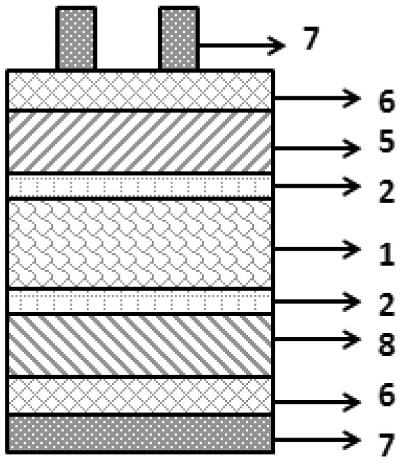
[0042] Such as figure 2 As shown, this embodiment provides a P-type double-sided multi-layer film fully passivated contact crystalline silicon solar cell. The battery structure is metal electrode / transparent conductive layer / N + poly-SiOx / SiOx / c-Si (P) / SiOx / P + poly-SiOx / transparent conductive layer / metal electrode. A P-type Czochralski single-crystal silicon wafer is used as a crystalline silicon substrate 1 with a thickness of 200 μm and a resistivity of 1-10 Ωcm, and the surface of the crystalline silicon substrate is chemically polished on both sides. Its preparation process is:

[0043] (1) Chemical cleaning of the crystalline silicon substrate 1 .

[0044] (2) Immerse the crystalline silicon substrate 1 in a hot nitric acid solution at 100°C for 28 minutes, the mass fraction of the nitric acid solution is 68%, and grow a layer on the front and back surfaces of the crystalline silicon substrate 1 by wet chemical oxidation method The silicon oxide lay...


PUM

PropertyMeasurementUnit
thicknessaaaaaaaaaa
thicknessaaaaaaaaaa
thicknessaaaaaaaaaa

Abstract

The invention relates to a preparation method of a multilayer film passivation contact structure and a full-passivation contact crystalline silicon solar cell. The preparation method comprises the following steps: growing a silicon oxide layer on the surface of a crystalline silicon substrate, depositing a layer of undoped initial crystalline silicon oxide film on the surface of the silicon oxide layer, then depositing a layer of heavily doped initial crystalline silicon oxide film, and finally performing high-temperature annealing and recrystallization to form the multi-layer thin film passivation contact structure comprising the tunneling oxide layer / polycrystalline silicon oxide thin film. As front passivation contact of a crystalline silicon cell, optical absorption of a crystalline silicon substrate is guaranteed, and optical response of the cell is improved. The method has higher thermal stability, in the high-temperature annealing process, the silicon oxide thin film protects the dielectric layer structure, and the passivation effect of oxidation driving is enhanced; the silicon oxide thin film blocks further diffusion of doped atoms, high-energy band bending caused by heavy doping is kept, and an annealing process window in the high-temperature annealing process is widened.

Description

technical field [0001] The invention relates to a solar cell, in particular to a preparation method of a multilayer film passivation contact structure and a fully passivation contact crystalline silicon solar cell. Background technique [0002] In order to reduce the production cost of crystalline silicon solar cells, further improving the conversion efficiency of solar cells is still an effective means for the current photovoltaic industry. The contact recombination at the semiconductor-metal interface is a key issue that restricts the improvement of conversion efficiency. In the passivation contact technology scheme, the crystalline silicon heterojunction solar cell (HIT) has excellent interface passivation performance due to its intrinsic amorphous silicon film, and the surface of crystalline silicon has extremely low interfacial recombination, so that its open circuit voltage can reach 750mV. Combining interdigitated back contact (IBC) with amorphous silicon / crystallin...

Claims


Application Information

Patent Timeline
Patent Type & Authority Applications(China)
IPC IPC(8): H01L31/18C23C16/40C23C16/50C23C16/56C30B15/00C30B29/06C30B33/00
CPCH01L31/1868H01L31/1864H01L31/1872C30B29/06C30B15/00C30B33/005C23C16/50C23C16/401C23C16/56Y02P70/50Y02E10/50
Inventor 于威黄艳红贾丽哲刘林卿时晓萌刘啸宇路万兵丛日东
Owner HEBEI UNIVERSITY
Learn More