
N-type organic semiconductor material based on naphthalimide and thiophene and preparation method and application

A technology of organic semiconductor and naphthalimide, which is applied in the field of n-type organic semiconductor materials and its preparation, can solve the problems of light and oxygen instability, complex interface layer, high price, etc., and achieve excellent thermal stability, high electronic Effects of mobility, good absorbance

Pending Publication Date: 2022-01-21
NANJING UNIV OF POSTS & TELECOMM
View PDF1 Cites 1 Cited by
  • Summary
  • Abstract
  • Description
  • Claims
  • Application Information

AI Technical Summary

Problems solved by technology

In these devices, adopting a bilayer structure as the interfacial layer between perovskite and Ag is relatively complicated, as demonstrated by C 60 (40nm) and BCP (10nm) The 50nm thick interface layer needs to be prepared by high vacuum evaporation, the cost is high
PCBM or fullerene derivatives are expensive and unstable to light and oxygen for a long time

Method used


Image

  • N-type organic semiconductor material based on naphthalimide and thiophene and preparation method and application
  • N-type organic semiconductor material based on naphthalimide and thiophene and preparation method and application
  • N-type organic semiconductor material based on naphthalimide and thiophene and preparation method and application

Examples


Embodiment 1

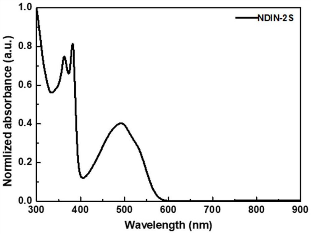
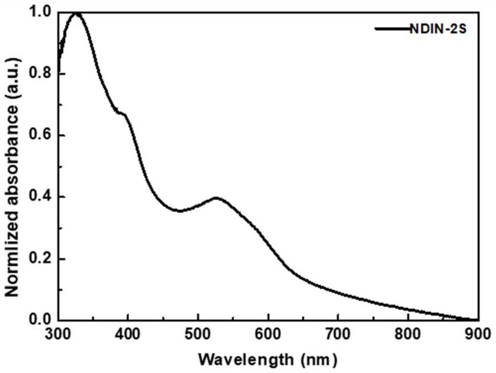
[0032] An n-type organic semiconductor material (NDIN-2S) based on naphthalimide and thiophene, its chemical structure is shown in formula I below:

[0033]

[0034] In Formula I: n is a natural number ranging from 1 to 12.

[0035] A method for preparing an n-type organic semiconductor material based on naphthalimide and thiophene, as shown in Reaction Formula II, the specific steps are as follows:

[0036]

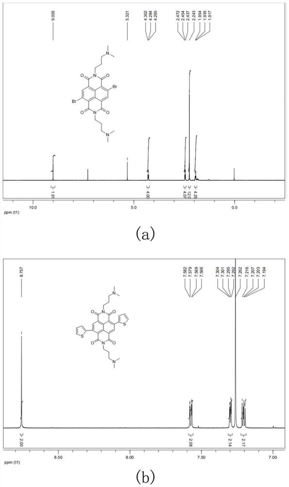
[0037](1) NDA-2Br(4,9-dibromo-2,7-bis(3-(dimethylamino)propyl)benzo[lmn][3,8]phenanthroline-1,3,6 ,8(2H,7H)-tetraketone) and N,N-dimethyl-propylenediamine are added to the reaction vessel at a molar ratio of 1:3, and HOAc (acetic acid) is used as a solvent, and an inert gas is passed through to discharge The air in the reaction vessel was refluxed at 130°C for 10 h; then the reaction mixture was distilled off under reduced pressure to remove HOAc, and then washed with Na 2 CO 3 Neutralized to weakly alkaline, extracted with dichloromethane, dried over anhydrous ...

Embodiment 2

[0043] The n-type organic semiconductor material (NDIN-2S) based on naphthalimide and thiophene obtained in Example 1 is used to prepare a perovskite solar cell device, and the specific steps are as follows:

[0044] (1) Clean the purchased indium tin oxide (ITO) glass with detergent first, and then ultrasonically clean it with tap water, deionized water, ethanol, acetone, and isopropanol in sequence.

[0045] (2) Spin-coat a 20nm-thick hole-transport layer NiO after drying the ITO for later use.

[0046] (3) Preparation of 200 nm thick CH on the NiO layer 3 NH 3 PbCl 0.1 I 2.9 perovskite layer.

[0047] (3) Spin-coat NDIN-2S on the perovskite layer to form a 1-5nm thick cathode modification layer, and the effective area of ​​the active layer of the solar device is 7.2mm 2 . ;

[0048] (4) In vacuum (4×10 -4 80nm-thick metal Ag was vapor-deposited under Pa) environment as the cathode electrode.

[0049] A Newport 500W xenon lamp equipped with an AM1.5 filter was used ...


PUM

PropertyMeasurementUnit
thicknessaaaaaaaaaa
thicknessaaaaaaaaaa

Abstract

The invention discloses an n-type organic semiconductor material based on naphthalimide and thiophene and a preparation method and application. The chemical structural formula of the n-type organic semiconductor material is shown as a formula I in the specification. Naphthalimide with plane rigidity is used as a strong electron-withdrawing unit, a thiophene derivative with strong conductivity is used as an electron-donating unit, an organic small molecule n-type semiconductor material (NDIN-2S) is formed, structures of the polymers and intermediates thereof are represented by nuclear magnetism and mass spectrometry, and photophysical properties of the polymers are represented by an ultraviolet visible spectrophotometer; and the thermal stability is analyzed through thermogravimetric analysis. Results show that the material has high electron mobility, good light absorption, excellent thermal stability and appropriate energy level, and is an ideal perovskite solar cell cathode modification layer material.

Description

technical field [0001] The invention belongs to the technical field of semiconductor materials, and in particular relates to an n-type organic semiconductor material based on naphthalimide and thiophene, its preparation method and application. Background technique [0002] Solar energy is an inexhaustible clean and green energy. In recent years, with the attention of countries all over the world on energy issues, solar cells have become a research hotspot in this field. Compared with traditional semiconductor solar cells, perovskite solar cells have outstanding advantages such as low cost, high efficiency, simple manufacturing process, and can be fabricated into flexible devices, and have broad development and application prospects. At present, the efficiency of perovskite solar cells has exceeded 25%, which fully meets the needs of commercialization, but stability is still an important issue for mass production and commercial use. As an important functional layer that extr...

Claims


Application Information

Patent Timeline
Patent Type & Authority Applications(China)
IPC IPC(8): C07D471/06H01L51/46H01L51/42
CPCC07D471/06H10K85/655H10K85/6572Y02E10/549
Inventor 虞惠闫伟博辛颢范浩
Owner NANJING UNIV OF POSTS & TELECOMM
Learn More